2. MIPI User Guide
2.1. Overview
MIPI Rx can receive the signal of differential and DC(TTL) interface, convert the data into pixel data, and then transfer it to ISP module. Differential signal supports video input such as SubLVDS(Sub Low-Voltage Differential Signal), MIPI-CSI and HiSPi(High-Speed Serial Pixel Interface). DC signal supports Sensor RAW12, BT1120, BT656 and BT601.
2.2. Important Concept
MIPI
MIPI (Mobile Industry Processor Interface) is a communication interface that uses D-PHY transmission specification and CSI-2 as protocol layer in physical layer.
Lane
The physical layer is used to connect a pair of high-speed differential lines between the sender and the receiver. A lane can transmit clock or data. 1C4D refers to one clock lane and four data lanes.
LVDS
Low voltage differential signaling (LVDS) refers to sub LVDS and HiSPi, which are developed from LVDS. The blanking zone and effective data are distinguished by synchronization code.
Synchronization Code
MIPI-CSI uses standard short packets as synchronization signals. LVDS signal uses sync code as synchronization signal. LVDS has two synchronization modes:
Use SOF/EOF to indicate the beginning and end of a frame.
Use SOL/EOL to indicate the beginning and end of the line.

Fig. 2.1 synchronization mode of SOF/EOF/SOL/EOL
Use SAV invalid and EAV invalid indicate the beginning and end of VBLANK.
Use SAV valid and EAV valid indicate the beginning and end of the effective information (information line, H.OB and pixel data).

Fig. 2.2 SAV/EAV synchronization mode
DOL
Sony’s interleaved WDR mode is called digital overlap.
2.3. Function Description
MIPI RX supports differential video input interfaces of MiPI-CSI, sub-LVDS and HiSPi which having one channel of up to 4 lanes or two channels of up to 2 lanes, besides, these interfaces support lane interchange and PN interchange of differential signals. Note that if two input channels of the differential signal are used, the number of pin MIPIRX# must be divided into 0-2 and 3-5 with each group receiving the same input. MIPI RX also supports sensor TTL, BT1120, BT656 and BT601 parallel input interfaces, and supports lane function interchange except Clock lane. The specific lane distribution is shown in the table below :
VI0 |
PAD NAME |
VI1 |
PAD NAME |
VI2 |
PAD NAME |
|---|---|---|---|---|---|
VI0_CLOCK |
MIPIRX4N |
V CLOCK |
V _CLOCK |
V CLOCK |
V _CLOCK |
VI0_D[0] |
MIPIRX4P |
||||
VI0_D[1] |
MIPIRX3N |
||||
VI0_D[2] |
MIPIRX3P |
||||
VI0_D[3] |
MIPIRX2N |
||||
VI0_D[4] |
MIPIRX2P |
||||
VI0_D[5] |
MIPIRX1N |
||||
VI0_D[6] |
MIPIRX1P |
||||
VI0_D[7] |
MIPIRX0N |
||||
VI0_D[8] |
MIPIRX0P |
||||
VI0_D[9] |
M IPI_TXM0 |
||||
VI0_D[10] |
M IPI_TXP0 |
V D[10] |
|||
VI0_D[11] |
M IPI_TXM1 |
V D[11] |
|||
VI0_D[12] |
M IPI_TXP1 |
V D[12] |
|||
VI0_D[13] |
M IPI_TXM2 |
V D[13] |
|||
VI0_D[14] |
M IPI_TXP2 |
V D[14] |
|||
V D[15] |
|||||
V D[16] |
|||||
V D[17] |
|||||
V D[18] |
MIPI RX supports the demultiplexing of MIPI-CSI and can receive channel information from different channel ID.
Fig. 2.3 The channel ID of MIPI-CSI
MIPI RX supports the demultiplexing of BT interfaces. The input end packages information coming from different channels in BT656 format. MIPI RX can restore each channel and then solve the valid data with the corresponding synchronization code. Note that this mode only supports SDR.
Fig. 2.4 The input with the support of BT demux mode
2.4. API Reference
MIPI Rx provides the function of docking sensor timing. The IOCTL interface is provided. The available commands are as follows:
CVI_MIPI_SET_HS_MODE Set the Lane distribution mode of MIPI.
CVI_MIPI_SET_DEV_ATTR: Set MIPI and parallel device properties.
CVI_MIPI_RESET_SENSOR: Reset the sensor.
CVI_MIPI_UNRESET_SENSOR: Undo reset the sensor.
CVI_MIPI_RESET_MIPI: Reset MIPI Rx.
CVI_MIPI_ENABLE_SENSOR_CLOCK: Turn on the CLOCK of SENSOR.
CVI_MIPI_DISABLE_SENSOR_CLOCK: Turn off the CLOCK of SENSOR.
CVI_MIPI_SET_CROP_TOP: Discard the first N data in each frame
CVI_MIPI_SET_WDR_MANUAL: Turn on the WDR manual mode.
CVI_MIPI_SET_LVDS_FP_VS: Set the time point of VSYNC generated in LVDS.
MIPI Tx provides the function of docking display and cascading.
The single OS provides an ioctl interface. The available commands are as follows:
CVI_VIP_MIPI_TX_SET_DEV_CFG : Set the properties of the MIPI Tx device.
CVI_VIP_MIPI_TX_GET_CMD : Read information from MIPI Tx device.
CVI_VIP_MIPI_TX_SET_CMD : The device send command to MIPI Tx device.
CVI_VIP_MIPI_TX_ENABLE : Enable MIPI Tx device.
CVI_VIP_MIPI_TX_DISABLE : Disable MIPI Tx device.
CVI_VIP_MIPI_TX_SET_HS_SETTLE : Set the settle timing of MIPI Tx in HS mode.
CVI_VIP_MIPI_TX_GET_HS_SETTLE : obtain the settle timing of MIPI Tx in HS mode.
The dual OS provides an ioctl interface. The available commands are as follows:
MSG_CMD_MIPI_TX_SET_DEV_CFG: Set the properties of the MIPI Tx device.
MSG_CMD_MIPI_TX_GET_CMD: Read information from MIPI Tx device.
MSG_CMD_MIPI_TX_SET_CMD: The device send command to MIPI Tx device.
MSG_CMD_MIPI_TX_ENABLE: Enable MIPI Tx device.
MSG_CMD_MIPI_TX_DISABLE: Disable MIPI Tx device.
MSG_CMD_MIPI_TX_SET_HS_SETTLE: Set the settle timing of MIPI Tx in HS mode.
MSG_CMD_MIPI_TX_GET_HS_SETTLE: obtain the settle timing of MIPI Tx in HS mode.
2.4.1. CVI_MIPI_SET_HS_MODE
【Description】
Relating functions are replaced by CVI_MIPI_SET_DEV_ATTR.
2.4.2. CVI_MIPI_SET_DEV_ATTR
【Description】
Set MIPI and parallel device properties.
【Parameter】
#define CVI_MIPI_SET_DEV_ATTR _IOW(CVI_MIPI_IOC_MAGIC, 0x01, struct combo_dev_attr_t)
【Syntax】
Pointer of type struct combo_dev_attr_t
【Return Value】
Return Value |
Description |
|---|---|
0 |
Success |
-1 |
Failure, please refer to the error code. |
【Processor Difference】
None
【Requirement】
Header files: cvi_vip_cif.h
【Note】
Before configuring CVI_MIPI_SET_DEV_ATTR, you need to use ISP interface to turn on the CLOCK of MIPI_RX. Please refer to ISP related documents for details.
Before configuring CVI_MIPI_SET_DEV_ATTR, the following interfaces need to be configured:
Reset MIPI: the interface is CVI_MIPI_RESET_MIPI.
Turn on the CLOCK of Sensor: the interface is CVI_MIPI_ENABLE_SENSOR_CLOCK.
Reset Sensor: the interface is CVI_MIPI_RESET_SENSOR.
Undo reset Sensor: the interface is CVI_MIPI_UNRESET_SENSOR.
The recommended configuration process are as follows:
Turn on the CLOCK of ISP.
Reset the docking Sensor.
Reset MIPI Rx.
Configure MIPI Rx device properties.
Turn on all clocks connected to Sensor.
Undo reset the docking Sensor.
The recommended exit process are as follows:
Reset the docking Sensor.
Turn off all the clock connected to the Sensor.
Reset MIPI Rx.
Turn off the CLOCK of ISP.
Operating the sensor reset signal line and clock signal line will have an effect on all sensors connected to the signal line.
【Related data types and Interfaces】
CVI_MIPI_RESET_MIPI
CVI_MIPI_ENABLE_SENSOR_CLOCK
CVI_MIPI_DISABLE_SENSOR_CLOCK
CVI_MIPI_RESET_SENSOR
CVI_MIPI_UNRESET_SENSOR
CVI_MIPI_RESET_SENSOR
2.4.3. CVI_MIPI_RESET_SENSOR
【Description】
Reset sensor
【Syntax】
#define CVI_MIPI_RESET_SENSOR _IOW(CVI_MIPI_IOC_MAGIC, 0x05, unsigned int)
【Parameter】
unsigned int. Sensor reset signal line number.
【Return Value】
Return Value |
Description |
|---|---|
0 |
Success |
-1 |
Failure, please refer to the error code. |
【Processor Difference】
None
【Requirement】
Header files: cvi_vip_cif.h
【Note】
The sensor reset signal is bound to the corresponding dts.
mipi_rx: cif {
compatible = "cvitek,cif";
reg = <0x0 0x0a0c2000 0x0 0x2000>, <0x0 0x0a0d0000 0x0 0x1000>,
<0x0 0x0a0c4000 0x0 0x2000>;
reg-names = "csi_mac0", "csi_wrap0", "csi_mac1";
interrupts = <GIC_SPI 155 IRQ_TYPE_LEVEL_HIGH>,
            <GIC_SPI 156 IRQ_TYPE_LEVEL_HIGH>;
interrupt-names = "csi0", "csi1";
snsr-reset = <&porta 2 GPIO_ACTIVE_LOW>, <&porta 2 GPIO_ACTIVE_LOW>;
resets = <&rst RST_CSIPHY0>, <&rst RST_CSIPHY1>,
<&rst RST_CSIPHY0RST_APB>, <&rst RST_CSIPHY1RST_APB>;
reset-names = "phy0", "phy1", "phy-apb0", "phy-apb1";
clocks = <&clock CV181X_CLOCK_CAM0>, <&clock CV181X_CLOCK_CAM1>, <&clock CV181X_CLOCK_SRC_VIP_SYS_2>;
clock-names = "clock_cam0", "clock_cam1", "clock_sys_2";
};
2.4.4. CVI_MIPI_UNRESET_SENSOR
【Description】
Undo reset sensor.
【Syntax】
#define CVI_MIPI_UNRESET_SENSOR _IOW(CVI_MIPI_IOC_MAGIC, 0x06, unsigned int)
【Parameter】
unsigned int. Sensor reset signal line number.
【Return Value】
Return Value |
Description |
|---|---|
0 |
Success |
-1 |
Failure, please refer to the error code. |
【Processor Difference】
None
【Requirement】
Header files:cvi_vip_cif.h
【Note】
The sensor reset signal is bound to the corresponding dts.
mipi_rx: cif {
compatible = "cvitek,cif";
reg = <0x0 0x0a0c2000 0x0 0x2000>, <0x0 0x0a0d0000 0x0 0x1000>,
<0x0 0x0a0c4000 0x0 0x2000>;
reg-names = "csi_mac0", "csi_wrap0", "csi_mac1";
interrupts = <GIC_SPI 155 IRQ_TYPE_LEVEL_HIGH>,
            <GIC_SPI 156 IRQ_TYPE_LEVEL_HIGH>;
interrupt-names = "csi0", "csi1";
snsr-reset = <&porta 2 GPIO_ACTIVE_LOW>, <&porta 2 GPIO_ACTIVE_LOW>;
resets = <&rst RST_CSIPHY0>, <&rst RST_CSIPHY1>,
<&rst RST_CSIPHY0RST_APB>, <&rst RST_CSIPHY1RST_APB>;
reset-names = "phy0", "phy1", "phy-apb0", "phy-apb1";
clocks = <&clock CV181X_CLOCK_CAM0>, <&clock CV181X_CLOCK_CAM1>, <&clock CV181X_CLOCK_SRC_VIP_SYS_2>;
clock-names = "clock_cam0", "clock_cam1", "clock_sys_2";
};
2.4.5. CVI_MIPI_RESET_MIPI
【Description】
Reset MIPI_Rx.
【Syntax】
#define CVI_MIPI_RESET_MIPI _IOW(CVI_MIPI_IOC_MAGIC, 0x07, unsigned int)
【Parameter】
unsigned int. MIPI_RX device number.
【Return Value】
Return Value |
Description |
|---|---|
0 |
Success |
-1 |
Failure, please refer to the error code. |
【Processor Difference】
None
【Requirement】
Header files:cvi_vip_cif.h
【Note】
2.4.6. CVI_MIPI_ENABLE_SENSOR_CLOCK
【Description】
Turn on the sensor clock.
【Syntax】
#define CVI_MIPI_ENABLE_SENSOR_CLOCK _IOW(CVI_MIPI_IOC_MAGIC, 0x10, unsigned int)
【Parameter】
unsigned int. MIPI_Rx device number.
【Return Value】
Return Value |
Description |
|---|---|
0 |
Success |
-1 |
fail and set errno |
【Processor Difference】
none
【Requirement】
Header files: cvi_vip_cif.h
【Note】
2.4.7. CVI_MIPI_DISABLE_SENSOR_CLOCK
【Description】
Turn off the clock of sensor.
【Syntax】
#define CVI_MIPI_DISABLE_SENSOR_CLOCK _IOW(CVI_MIPI_IOC_MAGIC, 0x11, unsigned int)
【Parameter】
unsigned int.MIPI_Rx device number。
【Return Value】
Return Value |
Description |
|---|---|
0 |
Success |
-1 |
Failure, please refer to the error code. |
【Processor Difference】
none
【Requirement】
Header files: cvi_vip_cif.h
【Note】
2.4.8. CVI_MIPI_SET_CROP_TOP
【Description】
Discard the first n data in each frame
【Syntax】
#define CVI_MIPI_SET_WDR_MANUAL _IOW(CVI_MIPI_IOC_MAGIC, 0x21, struct crop_top_s)
【Parameter】
struct crop_top_s
【Return Value】
Return Value |
Description |
|---|---|
0 |
Success |
-1 |
fail and seterrno |
【Processor Difference】
none
【Requirement】
Header files: cvi_vip_cif.h
【Note】
2.4.9. CVI_MIPI_SET_WDR_MANUAL
【Description】
Turn on WDR manual mode.
【Syntax】
#define CVI_MIPI_SET_WDR_MANUAL _IOW(CVI_MIPI_IOC_MAGIC, 0x21, struct manual_wdr_s)
【Parameter】
struct manual_wdr_s
【Return Value】
Return Value |
Description |
|---|---|
0 |
Success |
-1 |
Failure, please refer to the error code. |
【Processor Difference】
none
【Requirement】
Header files: cvi_vip_cif.h
【Note】
2.4.10. CVI_MIPI_SET_LVDS_FP_VS
【Description】
Set the time point of VSYNC generation in sub-LVDS
【Syntax】
#define CVI_MIPI_SET_LVDS_FP_VS _IOW(CVI_MIPI_IOC_MAGIC, 0x22, struct vsync_gen_s)
【Parameter】
struct vsync_gen_s
【Return Value】
Return Value |
Description |
|---|---|
0 |
Success |
-1 |
fail and seterrno |
【Processor Difference】
none
【Requirement】
Header files: cvi_vip_cif.h
【Note】
2.4.11. CVI_VIP_MIPI_TX_SET_DEV_CFG
【Description】
Set the properties of the MIPI Tx device.
【Syntax】
#define CVI_VIP_MIPI_TX_SET_DEV_CFG _IOW(CVI_VIP_MIPI_TX_IOC_MAGIC, 0x01, struct combo_dev_cfg_s)
【Parameter】
MIPI Tx device properties, See the Description of combo_dev_cfg_s structure for details.
【Return Value】
Return Value |
Description |
|---|---|
0 |
Success |
-1 |
Failure, please refer to the error code. |
【Processor Difference】
none
【Requirement】
Header files: cvi_mipi_tx.h
【Note】
2.4.12. MSG_CMD_MIPI_TX_SET_DEV_CFG
The description, parameters, return value, processor difference, requirement, and note of this dual OS are the same as those of the single OS command CVI_VIP_MIPI_TX_SET_DEV_CFG.
【Syntax】
typedef enum tagMSG_MIPI_TX_CMD_E {
    MSG_CMD_MIPI_TX_SET_DEV_CFG = 0,
    MSG_CMD_MIPI_TX_SET_CMD,
    MSG_CMD_MIPI_TX_GET_CMD,
    MSG_CMD_MIPI_TX_ENABLE,
    MSG_CMD_MIPI_TX_DISABLE,
    MSG_CMD_MIPI_TX_SET_HS_SETTLE,
    MSG_CMD_MIPI_TX_GET_HS_SETTLE,
    MSG_CMD_MIPI_TX_BUFF
} MSG_MIPI_TX_CMD_E;
The definitions of subsequent commands for dual OS come from this enumeration and will not be described again.
2.4.13. CVI_VIP_MIPI_TX_GET_CMD
【Description】
Read information from MIPI Tx device.
【Syntax】
#define CVI_VIP_MIPI_TX_GET_CMD _IOWR(CVI_VIP_MIPI_TX_IOC_MAGIC, 0x04, struct get_cmd_info_s)
【Parameter】
See the Description of get_cmd_info_s structure for details.
【Return Value】
Return Value |
Description |
|---|---|
0 |
Success |
-1 |
Failure, please refer to the error code. |
【Processor Difference】
processor type |
support or not |
|---|---|
CV1835 |
support,get_data_size max 4 |
【Requirement】
Header files: cvi_mipi_tx.h
【Note】
2.4.14. MSG_CMD_MIPI_TX_GET_CMD
The description, parameters, return value, processor difference, requirement, and note of this dual OS are the same as those of the single OS command CVI_VIP_MIPI_TX_GET_CMD.
【Syntax】
See the Description of MSG_CMD_MIPI_TX_SET_DEV_CFG command for details.
2.4.15. CVI_VIP_MIPI_TX_SET_CMD
【Description】
The device sends commands to the MIPI Tx device.
【Syntax】
#define CVI_VIP_MIPI_TX_SET_CMD _IOW(CVI_VIP_MIPI_TX_IOC_MAGIC, 0x02, struct cmd_info_s)
【Parameter】
See the Description of cmd_info_s structure for details.
【Return Value】
Return Value |
Description |
|---|---|
0 |
Success |
-1 |
Failure, please refer to the error code. |
【Processor Difference】
None
【Requirement】
Header files: cvi_mipi_tx.h
【Note】
2.4.16. MSG_CMD_MIPI_TX_SET_CMD
The description, parameters, return value, processor difference, requirement, and note of this dual OS are the same as those of the single OS command CVI_VIP_MIPI_TX_SET_CMD.
【Syntax】
See the Description of MSG_CMD_MIPI_TX_SET_DEV_CFG command for details.
2.4.17. CVI_VIP_MIPI_TX_ENABLE
【Description】
Enable Mipi TX device.
【Syntax】
#define CVI_VIP_MIPI_TX_ENABLE _IO(CVI_VIP_MIPI_TX_IOC_MAGIC, 0x03)
【Parameter】
none
【Return Value】
Return Value |
Description |
|---|---|
0 |
Success |
-1 |
Failure, please refer to the error code. |
【Processor Difference】
None
【Requirement】
Header files: cvi_mipi_tx.h
【Note】
After this API call, mipi will switch to HS mode.
2.4.18. MSG_CMD_MIPI_TX_ENABLE
The description, parameters, return value, processor difference, requirement, and note of this dual OS are the same as those of the single OS command CVI_VIP_MIPI_TX_ENABLE.
【Syntax】
See the Description of MSG_CMD_MIPI_TX_SET_DEV_CFG command for details.
2.4.19. CVI_VIP_MIPI_TX_DISABLE
【Description】
Disable MIPI Tx device.
【Syntax】
#define CVI_VIP_MIPI_TX_DISABLE _IO(CVI_VIP_MIPI_TX_IOC_MAGIC, 0x05)
【Parameter】
none
【Return Value】
Return Value |
Description |
|---|---|
0 |
success |
-1 |
Failure, please refer to the error code. |
【Processor Difference】
None
【Requirement】
Header files: cvi_mipi_tx.h
【Note】
After this API call, mipi will switch to LP mode.
2.4.20. MSG_CMD_MIPI_TX_DISABLE
The description, parameters, return value, processor difference, requirement, and note of this dual OS are the same as those of the single OS command CVI_VIP_MIPI_TX_DISABLE.
【Syntax】
See the Description of MSG_CMD_MIPI_TX_SET_DEV_CFG command for details.
2.4.21. CVI_VIP_MIPI_TX_SET_HS_SETTLE
【Description】
Set the settle timing of MIPI Tx in HS mode.
【Syntax】
#define CVI_VIP_MIPI_TX_SET_HS_SETTLE _IOW(CVI_VIP_MIPI_TX_IOC_MAGIC, 0x06, struct hs_settle_s)
【Parameter】
See the Description of hs_settle_s structure for details.
【Return Value】
Return Value |
Description |
|---|---|
0 |
Success |
-1 |
Failure, please refer to the error code. |
【Processor Difference】
None
【Requirement】
Header files: cvi_mipi_tx.h
【Note】
2.4.22. MSG_CMD_MIPI_TX_SET_HS_SETTLE
The description, parameters, return value, processor difference, requirement, and note of this dual OS are the same as those of the single OS command CVI_VIP_MIPI_TX_SET_HS_SETTLE.
【Syntax】
See the Description of MSG_CMD_MIPI_TX_SET_DEV_CFG command for details.
2.4.23. CVI_VIP_MIPI_TX_GET_HS_SETTLE
【Description】
Get the settle timing of MIPI Tx in HS mode.
【Syntax】
#define CVI_VIP_MIPI_TX_GET_HS_SETTLE _IOWR(CVI_MIPI_TX_IOC_MAGIC, 0x06, struct hs_settle_s)
【Parameter】
See the Description of hs_settle_s structure for details.
【Return Value】
Return Value |
Description |
|---|---|
0 |
Success |
-1 |
Failure, please refer to the error code. |
【Processor Difference】
None
【Requirement】
Header files: cvi_mipi_tx.h
【Note】
2.4.24. MSG_CMD_MIPI_TX_GET_HS_SETTLE
The description, parameters, return value, processor difference, requirement, and note of this dual OS are the same as those of the single OS command CVI_VIP_MIPI_TX_GET_HS_SETTLE.
【Syntax】
See the Description of MSG_CMD_MIPI_TX_SET_DEV_CFG command for details.
2.5. Data Types
The Syntax of MIPI RX data type is as follows:
CVI_MIPI_IOC_MAGIC: Magic number of MIPI Rx ioctl command.
MIPI_LANE_NUM: The maximum number of lanes supported by MIPI devices of MIPI Rx.
WDR_VC_NUM: define the maximum number of supported Virtual Channels.
SYNC_CODE_NUM: Defines the number of synchronization codes for each virtual channel of LVDS.
input_mode_e: MIPI Rx input interface type.
img_size_s: The size of each frame of MIPI Rx input data.
rx_mac_clock_e: the working clock supported by MAC.
cam_pll_freq_e: The sensor reference clock of MIPI-RX output.
mclock_pll_s: Sensor reference clock setting of MIPI-RX output.
raw_data_type_e: MIPI Rx input data format.
mipi_wdr_mode_e: MIPI-CSI WDR mode.
wdr_mode_e: LVDS/HISPI WDR mode.
lvds_sync_mode_e: LVDS synchronization mode.
lvds_bit_endian: Big endian mode.
lvds_vsync_type_e: The synchronization mode of LVDS in WDR mode.
lvds_fid_type_e: LVDS frame identification ID type.
lvds_fid_type_s: LVDS frame identification ID type.
lvds_vsync_type_s: LVDS WDR synchronization Parameter.
lvds_dev_attr_s: SubLVDS/HiSPi device properties.
dphy_s: the properties of MIPI DPHY.
mipi_demux_info_s: the properties of MIPI in demultiplexing mode.
mipi_dev_attr_s: MIPI-CSI device properties.
manual_wdr_attr_s: Manual WDR mode Parameter.
ttl_pin_func_e: the config function of TTL/BT interfaces.
ttl_src_e: the input source of TTL/BT interfaces.
bt_demux_mode_e: the number of channels of BT in demultiplexing mode.
bt_demux_sync_s: the synchronization code config of BT in demultiplexing mode.
bt_demux_attr_s: the device properties of BT in demultiplexing mode.
ttl_dev_attr_s: the TTL/BT devices’properties.
combo_dev_attr_s: combo device properties.
crop_top_s: Discard the row data attribute at the beginning.
manual_wdr_s: Manual WDR mode setting.
vsync_gen_s: SUBLVDS Vertical synchronization signal properties.
The Syntax of MIPI RX data type is as follows:
LANE_MAX_NUM: Maximum number of lanes supported by a MIPI Tx device.
output_mode_e: MIPI Tx output mode
video_mode_e: MIPI Tx video mode
output_format_e: MIPI Tx output format
sync_info_s: MIPI Tx device synchronization information
combo_dev_cfg_s: MIPI Tx device properties
cmd_info_s: Retrieve information from MIPI Tx device
get_cmd_info_s: Retrieve information from MIPI Tx device
hs_settle_s: the information of settle of MIPI Tx devices in HS mode.
2.5.1. CVI_MIPI_IOC_MAGIC
【Description】
MIPI Rx ioctl magic number of command
【Syntax】
#define CVI_MIPI_IOC_MAGIC 'm'
【Processor Difference】
none.
【Note】
none.
【Related Data Type and Interface】
none
2.5.2. MIPI_LANE_NUM
【Description】
The maximum number of lanes supported by a MIPI Rx device.
【Syntax】
#define MIPI_LANE_NUM 4
【Processor Difference】
none.
【Note】
none.
【Related Data Type and Interface】
none
2.5.3. WDR_VC_NUM
【Description】
Define the maximum number of virtual channels supported
【Definition】
#define WDR_VC_NUM 2
【Processor Difference】
none.
【Note】
none.
【Related Data Type and Interface】
none
2.5.4. SYNC_CODE_NUM
【Description】
Defines the number of synchronization codes for each virtual channel of LVDS.
【Definition】
#define SYNC_CODE_NUM 4
【Processor Difference】
none.
【Note】
none.
【Related Data Type and Interface】
none
2.5.5. BT_DEMUX_NUM
【Description】
Define the maximum number of channels supported when using bt demux function.
【Definition】
#define BT_DEMUX_NUM 4
【Processor Difference】
none.
【Note】
none.
【Related Data Type and Interface】
none
2.5.6. MIPI_DEMUX_NUM
【Definition】
Defines the maximum number of virtual channels supported when using the mipi demux function.
【Definition】
#define MIPI_DEMUX_NUM 4
【Processor Difference】
none.
【Note】
none.
【Related Data Type and Interface】
none
2.5.7. input_mode_e
【Description】
MIPI Rx input interface type.
【Definition】
enum input_mode_e {
     INPUT_MODE_MIPI = 0,
     INPUT_MODE_SUBLVDS,
     INPUT_MODE_HISPI,
     INPUT_MODE_CMOS,
     INPUT_MODE_BT1120,
     INPUT_MODE_BT601_19B_VHS,
     INPUT_MODE_BT656_9B,
     INPUT_MODE_CUSTOM_0,
     INPUT_MODE_BT_DEMUX,
     INPUT_MODE_BUTT
};
【Processor Difference】
none.
【Note】
none.
【Related Data Type and Interface】
none
2.5.8. img_size_s
【Description】
The size of each frame of MIPI Rx input data.
【Definition】
struct img_size_s {
     unsigned int    width;
     unsigned int    height;
};
【Processor Difference】
none.
【Note】
none.
【Related Data Type and Interface】
none
2.5.9. rx_mac_clock_e
【Description】
MAC supports working clock.
【Definition】
enum rx_mac_clock_e {
     RX_MAC_CLOCK_200M = 0,
RX_MAC_CLOCK_400M,
     RX_MAC_CLOCK_500M,
RX_MAC_CLOCK_600M,
RX_MAC_CLOCK_BUTT,
};
【Processor Difference】
none.
【Note】
Please refer to 1.7.2 for the relationship between MAC clock and MIPI clock.
【Related Data Type and Interface】
none
2.5.10. cam_pll_freq_e
【Description】
The sensor reference clock of MIPI-RX output.
【Definition】
enum cam_pll_freq_e {
   CAMPLL_FREQ_NONE = 0,
   CAMPLL_FREQ_37P125M,
   CAMPLL_FREQ_25M,
   CAMPLL_FREQ_27M,
   CAMPLL_FREQ_24M,
   CAMPLL_FREQ_26M,
   CAMPLL_FREQ_NUM
};
【Processor Difference】
none.
【Note】
none.
【Related Data Type and Interface】
none
2.5.11. mclock_pll_s
【Description】
Sensor reference clock setting of MIPI-RX output.
【Definition】
struct mclock_pll_s {
   unsigned int      cam;
   enum cam_pll_freq_e   freq;
};
【Member】
Member |
Description |
|---|---|
cam |
0: output is CAM_MCLOCK0 1: output is CAM_MCLOCK1 |
freq |
The output reference Sensor clocktion |
【Processor Difference】
none
【Note】
none
【Related Data Type and Interface】
none
2.5.12. raw_data_type_e
【Description】
MIPI Rx data format。
【Definition】
enum raw_data_type_e {
     RAW_DATA_8BIT = 0,
     RAW_DATA_10BIT,
     RAW_DATA_12BIT,
     YUV422_8BIT,    /* MIPI-CSI only */
     YUV422_10BIT,   /* MIPI-CSI only*/
     RAW_DATA_BUTT
};
【Processor Difference】
none.
【Note】
YUV422_8BIT and YUV422_10BIT are only supported in MIPI-CSI mode
【Related Data Type and Interface】
none
2.5.13. mipi_wdr_mode_e
【Description】
MIPI-CSI WDR mode。
【Definition】
enum mipi_wdr_mode_e {
     CVI_MIPI_WDR_MODE_NONE = 0,
     CVI_MIPI_WDR_MODE_VC,
     CVI_MIPI_WDR_MODE_DT,
     CVI_MIPI_WDR_MODE_DOL,
     CVI_MIPI_WDR_MODE_MANUAL,  /* SOI case */
     CVI_MIPI_WDR_MODE_BUTT
};
【Member】
Member |
Description |
|---|---|
CVI_MIPI_WDR_MODE_NONE |
Linear mode |
CVI_MIPI_WDR_MODE_VC |
MIPI-CSI Virtual Channel mode |
CVI_MIPI_WDR_MODE_DT |
MIPI-CSI Data Type mode |
CVI_MIPI_WDR_MODE_DOL |
Sony DOL LI mode |
CVI_MIPI_WDR_MODE_MANUAL |
WDR manual mode |
【Processor Difference】
none.
【Note】
CVI_MIPI_WDR_MODE_VC is suitable for the sensor that uses MIPI-CSI Virtual Channel ID to distinguish long exposure line and short exposure line.
CVI_MIPI_WDR_MODE_DT is suitable for sensors that use MIPI-CSI Data Type ID to distinguish long exposure line and short exposure line. Note that long exposure and short exposure must start and end at the same frame.
CVI_MIPI_WDR_MODE_DOL is suitable for using SONY MIPI-CSI Line Information mode.
CVI_MIPI_WDR_MODE_Manual uses custom rules to determine long exposure line and short exposure line.
【Related Data Type and Interface】
none
2.5.14. wdr_mode_e
【Description】
Sub-LVDS/HISPI WDR mode.
【Definition】
enum wdr_mode_e {
     CVI_WDR_MODE_NONE = 0,
     CVI_WDR_MODE_2F,
     CVI_WDR_MODE_3F,
     CVI_WDR_MODE_DOL_2F,
     CVI_WDR_MODE_DOL_3F,
     CVI_WDR_MODE_DOL_BUTT
};
【Member】
Member |
Description |
|---|---|
CVI_WDR_MODE_NONE |
Linear mode |
CVI_WDR_MODE_2F |
General double exposure WDR |
CVI_WDR_MODE_3F |
General three exposure WDR |
CVI_WDR_MODE_DOL_2F |
Sony DOL-2 WDR |
CVI_WDR_MODE_DOL_3F |
Sony DOL-3 WDR |
【Processor Difference】
none.
【Note】
CVI_WDR_MODE_2F is suitable for general MIPI-CSI/HiSPi interleaved WDR.
CVI_WDR_MODE_DOL_2F is suitable for Sony Sub-LVDS DOL-2 WDR.
CV181x dose not support CVI_WDR_MODE_3F and CVI_WDR_MODE_DOL_3F.
CV180X no support WDR mode.
【Related Data Type and Interface】
none
2.5.15. lvds_sync_mode_e
【Description】
LVDS synchronization mode.
【Definition】
enum lvds_sync_mode_e {
     LVDS_SYNC_MODE_SOF = 0,
     LVDS_SYNC_MODE_SAV,
     LVDS_SYNC_MODE_BUTT
};
【Member】
Member |
Description |
|---|---|
LVDS_SYNC_MODE_SOF |
SOF, EOF, SOL, EOL. please refer to figure 2-1 |
LVDS_SYNC_MODE_SAV |
Invalid SAV, invalid EAV, valid SAV, valid EAV. please refer to figure 2-2. |
【Processor Difference】
none.
【Note】
LVDS_SYNC_MODE_SOF is suitable for HiSPi Packetize-SP mode.
LVDS_SYNC_MODE_SAV is suitable for sub-LVDS and HiSPi Streaming-SP mode.
When input is INPUT_MODE_HISPI and the synchronization mode is LVDS_SYNC_MODE_SAV。 MIPI-Rx switches to HiSPi Streaming-SP mode.
【Related Data Type and Interface】
none
2.5.16. lvds_bit_endian
【Description】
Bit endian mode.
【Definition】
enum lvds_bit_endian {
       LVDS_ENDIAN_LITTLE = 0,
       LVDS_ENDIAN_BIG,
       LVDS_ENDIAN_BUTT
};
【Processor Difference】
none
【Note】
none
【Related Data Type and Interface】
none
2.5.17. lvds_vsync_type_e
【Description】
The synchronization mode of LVDS in WDR mode.
【Definition】
enum lvds_vsync_type_e {
       LVDS_VSYNC_NORMAL = 0,
       LVDS_VSYNC_SHARE,
       LVDS_VSYNC_HCONNECT,
       LVDS_VSYNC_BUTT
};
【Member】
Member |
Description |
|---|---|
LVDS_VSYNC_NORMAL |
Long and short exposure frames have independent SOF-EOF, SOL-EOL or invalid-SAV-invalid-EAV, valid SAV-valid EAV |
LVDS_VSYNC_SHARE |
Long and short exposure frames share a pair of SOF-EOF marks, and the first few lines of short exposure are filled with fixed values |
LVDS_VSYNC_HCONNECT |
The long and short exposure frames share a pair of SAV-EAV marks, and there is a fixed period of blanking between the long and short exposure frames. |
LVDS_VSYNC_NORMAL synchronization mode:
Fig. 2.5 LVDS_VSYNC_NORMAL synchronization mode.
LVDS_VSYNC_HCONNECT synchronization mode:
Fig. 2.6 LVDS_VSYNC_HCONNECT synchronization mode.
【Processor Difference】
none
【Note】
LVDS_VSYNC_NORMAL is suitable for SONY sub-LVDS DOL-2 pattern 1 and HiSPi Packtized-SP WDR mode.
LVDS_VSYNC_SHARE is suitable for HiSPi Streaming-SP WDR mode.
LVDS_VSYNC_HCONNECT is suitable for SONY sub-LVDS DOL-2 pattern 2.
【Related Data Type and Interface】
none
2.5.18. lvds_fid_type_e
【Description】
LVDS frame identification ID type.
【Definition】
enum lvds_fid_type_e {
     LVDS_FID_NONE = 0,
     LVDS_FID_IN_SAV,
     LVDS_FID_BUTT,
};
【Member】
Member |
Description |
|---|---|
LVDS_FID_NONE |
Do not use frame identification id |
LVDS_FID_IN_SAV |
The FID is inserted in the fourth field of the SAV. |
【Processor Difference】
none
【Note】
none
【Related Data Type and Interface】
none
2.5.19. lvds_fid_type_s
【Description】
LVDS frame identification ID type.
【Definition】
struct lvds_fid_type_s {
       enum lvds_fid_type_e            fid;
};
【Member】
Member |
Description |
|---|---|
fid |
Frame identification type in LVDS DOL mode |
【Processor Difference】
none
【Note】
none
【Related Data Type and Interface】
none
2.5.20. lvds_vsync_type_s
【Description】
LVDS WDR synchronize Parameter.
【Definition】
struct lvds_vsync_type_s {
       enum lvds_vsync_type_e  sync_type;
       unsigned short                  hblank1;
       unsigned short                  hblank2;
};
【Processor Difference】
none
【Note】
When sync_type is LVDS_VSYNC_HCONNECT, hblank1 and hblank2 should be configured to indicate the length of the blanking zone between long and short exposures.
【Related Data Type and Interface】
none
2.5.21. lvds_dev_attr_s
【Description】
LVDS/SubLVDS/HiSPi device properties.
【Definition】
 struct lvds_dev_attr_s {
        enum wdr_mode_e                 wdr_mode;
        enum lvds_sync_mode_e           sync_mode;
        enum raw_data_type_e            raw_data_type;
        enum lvds_bit_endian            data_endian;
        enum lvds_bit_endian            sync_code_endian;
        short                           lane_id[MIPI_LANE_NUM+1];
        short   sync_code[MIPI_LANE_NUM][WDR_VC_NUM+1][SYNC_CODE_NUM];
        struct lvds_vsync_type_s        vsync_type;
        struct lvds_fid_type_s          fid_type;
        char                            pn_swap[MIPI_LANE_NUM+1];
};
【Member】
Member |
Description |
|---|---|
wdr_mode |
WDR mode |
sync_mode |
LVDS synchronization mode |
raw_data_type |
Type of data transferred |
data_endian |
Data endian |
sync_code_endian |
Synchronization code size mode |
lane_id |
The corresponding relationship between sensor and MIPI RX Lane |
sync_code |
Each virtual channel has four synchronization codes. According to different synchronization modes, they represent the synchronization codes of SOF/EOF/ SOL/EOL or invalid SAV/invalid EAV/ valid SAV/valid EAV respectively. |
vsync_type |
vsync type, when wdr_mod is in DOL mode and sync_mode is in LVDS_SYNC_MODE_SAV, you need to configure the type of vsync |
fid_type |
Frame identification type |
pn_swap |
Positive/negative line exchange or not |
【Processor Difference】
none
【Note】
none
【Related Data Type and Interface】
none
2.5.22. dphy_s
【Description】
MIPI RX DPHY device properties.
【Definition】
struct mipi_dev_attr_s {
       unsigned char           enable;
       unsigned char           hs_settle;
};
【Member】
Member |
Description |
|---|---|
enable |
Turn on the property setting of MIPI RX DPHY. |
hs_settle |
hs settle time |
【Processor Difference】
none
【Note】
none
【Related Data Type and Interface】
none
2.5.23. mipi_demux_info_s
【Description】
MIPI CSI use the property setting of Virtual Channel demultiplexing.
【Definition】
struct mipi_demux_info_s {
     unsigned int                    demux_en;
     unsigned char                   vc_mapping[MIPI_DEMUX_NUM];
};
【Member】
Member |
Description |
|---|---|
demux_en |
Turn on mipi virtual channel demultiplexing. |
vc_mapping |
Set the corresponding relationship of ISP channel and mipi virtual channel. Such as vc_mapping = {0, 2, 3, 1}, ISP ch0 indicates vc=0; ch1 indicates vc=2; ch2 indicates vc=3; ch3 indicates vc=1. |
【Processor Difference】
none
【Note】
none
【Related Data Type and Interface】
none
2.5.24. mipi_dev_attr_s
【Description】
MIPI-CSI devices’ property.
【Definition】
struct mipi_dev_attr_s {
       enum raw_data_type_e            raw_data_type;
       short                           lane_id[MIPI_LANE_NUM+1];
       enum mipi_wdr_mode_e           wdr_mode;
       short                           data_type[WDR_VC_NUM];
       char                            pn_swap[MIPI_LANE_NUM+1];
};
【Member】
Member |
Description |
|---|---|
wdr_mode |
WDR mode |
raw_data_type |
The type of transmitted data. |
lane_id |
The corresponding relationship between the sender (sensor) and the receiver (MIPI Rx) lane. |
data_type |
When WDR mode is CVI_MIPI_WDR_MODE_DT, the corresponding data type of each WDR frames. |
pn_swap |
Whether Positive and negative line are swapped. |
【Processor Difference】
none
【Note】
none
【Related Data Type and Interface】
none
2.5.25. manaul_wdr_attr_s
【Description】
Manual WDR mode Parameter.
【Definition】
struct manaul_wdr_attr_s {
       unsigned int                    manual_en;
       unsigned short                  l2s_distance;
       unsigned short                  lsef_length;
       unsigned int                    discard_padding_lines;
       unsigned int                    update;
};
【Member】
Member |
Description |
|---|---|
manual_en |
Manual switch of WDR. |
l2s_distance |
The distance from the first long exposure to the first short exposure in a frame, the unit is the number of rows. |
lsef_length |
The number of long/short exposure lines. |
discard_padding_lines |
Whether the sensor outputs the padding line as a valid line. |
update |
Whether to force the settings to be updated. If not, the setting will wait for the next synchronization signal to be updated. |
【Processor Difference】
none
【Note】
When HiSPi is input and sync_type is LVDS_VSYNC_SHARE, need to turn on the manual WDR mode and set Parameter.
When MIPI-CSI is input and wdr mode is CVI_MIPI_WDR_MODE_MANUAL, need to turn on the manual WDR mode and set Parameter.
【Related Data Type and Interface】
none
2.5.26. ttl_pin_func_e
【Description】
The config functions of TTL/BT interface.
【Definition】
enum ttl_pin_func_e {
     TTL_PIN_FUNC_VS,
     TTL_PIN_FUNC_HS,
     TTL_PIN_FUNC_VDE,
     TTL_PIN_FUNC_HDE,
     TTL_PIN_FUNC_D0,
     TTL_PIN_FUNC_D1,
     TTL_PIN_FUNC_D2,
     TTL_PIN_FUNC_D3,
     TTL_PIN_FUNC_D4,
     TTL_PIN_FUNC_D5,
     TTL_PIN_FUNC_D6,
     TTL_PIN_FUNC_D7,
     TTL_PIN_FUNC_D8,
     TTL_PIN_FUNC_D9,
     TTL_PIN_FUNC_D10,
     TTL_PIN_FUNC_D11,
     TTL_PIN_FUNC_D12,
     TTL_PIN_FUNC_D13,
     TTL_PIN_FUNC_D14,
     TTL_PIN_FUNC_D15,
     TTL_PIN_FUNC_NUM,
};
【Processor Difference】
none
【Note】
none
【Related Data Type and Interface】
none
2.5.27. ttl_src_e
【Description】
The input source of TTL/BT interfaces.
【Definition】
enum ttl_src_e {
     TTL_VI_SRC_VI0 = 0,
     TTL_VI_SRC_VI1,
     TTL_VI_SRC_VI2,         /* BT demux */
     TTL_VI_SRC_NUM
};
【Processor Difference】
none
【Note】
none
【Related Data Type and Interface】
Please refer to the tabel 2-1.
2.5.28. bt_demux_mode_e
【Description】
The channels’ number of BT demultiplexing mode.
【Definition】
enum bt_demux_mode_e {
     BT_DEMUX_DISABLE = 0,
     BT_DEMUX_2,
     BT_DEMUX_3,
     BT_DEMUX_4,
};
【Processor Difference】
none
【Note】
none
【Related Data Type and Interface】
None
2.5.29. bt_demux_sync_s
【Description】
The synchronization code setting of BT demultiplexing mode.
【Definition】
struct bt_demux_sync_s {
     unsigned char           sav_vld;
     unsigned char           sav_blk;
     unsigned char           eav_vld;
     unsigned char           eav_blk;
};
【Member】
Member |
Description |
|---|---|
sav_vld |
The SAV of the valid data interval |
sav_blk |
The SAV of blank data interval. |
eav_vld |
The EAV of the valid data interval |
eav_blk |
The EAV of blank data interval. |
【Processor Difference】
none
【Note】
none
【Related Data Type and Interface】
None
2.5.30. bt_demux_attr_s
【Description】
The property setting of BT in demultiplexing mode.
【Definition】
struct bt_demux_attr_s {
     signed char                     func[TTL_PIN_FUNC_NUM];
     unsigned short                  v_fp;
     unsigned short                  h_fp;
     unsigned short                  v_bp;
     unsigned short                  h_bp;
     enum bt_demux_mode_e            mode;
     unsigned char                   sync_code_part_A[3];    /* sync code 0~2 */
     struct bt_demux_sync_s          sync_code_part_B[BT_DEMUX_NUM]; /* sync code 3 */
     char                            yc_exchg;
};
【Member】
Member |
Description |
|---|---|
func |
The corresponding input source of BT interface is the lane number of TTL_VI_SRC_VI2. Index is the logic function of BT, as for value please refer to table 1-1. Such as, func[TTL_PIN_FUNC_D0] = 5, indicates the BT signal’s D0 receive VI2_D[5], namely pad name VIVO_D5. |
v_fp |
The front porch in vertical direction |
h_fp |
The front porch in horizontal direction |
v_bp |
The back porch in vertical direction |
h_bp |
The back porch in horizontal direction |
mode |
The channel’s number of BT in demultiplexing mode. |
sync_code_part_A |
The synchronization code between 0~2 of BT in demultiplexing mode |
sync_code_part_B |
The BT demultiplexing mode’s synchronization code 3 |
yc_exchg |
BIT0 to BIT3 represent the sequence exchange of Y Cb/Cr bytes from CH0 to CH3, where 1 indicates the exchange and 0 indicates the non-exchange. |
【Processor Difference】
none
【Note】
none
【Related Data Type and Interface】
None
2.5.31. ttl_dev_attr_s
【Description】
The property setting of TTL/BT interface.
【Definition】
struct ttl_dev_attr_s {
     enum ttl_src_e                  vi;
     signed char                     func[TTL_PIN_FUNC_NUM];
     unsigned short                  v_bp;
     unsigned short                  h_bp;
};
【Member】
Member |
Description |
|---|---|
vi |
Input source of the TTL/BT interface. The allowed value is TTL_VI_SRC_VI0 or TTL_VI_SRC_VI1 |
func |
The BT interface is corresponding with the lane number of input source. Index is the logic function of BT, as for value please refer to label 1-1. Such as, when vi = TTL_VI_SRC_VI1, func[TTL_PIN_FUNC_D0] = 5, indicates BT signal’s D0 receive VI1_D[5], namely pad name VIVO_D5. |
v_bp |
The back porch in vertical direction |
h_bp |
The back porch in horizontal direction |
【Processor Difference】
none
【Note】
none
【Related Data Type and Interface】
None
2.5.32. combo_dev_attr_s
【Description】
Combo device properties, because MIPI Rx can interface with CSI-2, sub-LVDS, HiSPi and other time sequences, MIPI Rx is called a combo device.
【Definition】
struct combo_dev_attr_s {
      enum input_mode_e            input_mode;
      enum rx_mac_clock_e             mac_clock;
      struct mclock_pll_s                mclock;
      union {
              struct mipi_dev_attr_s  mipi_attr;
              struct lvds_dev_attr_s  lvds_attr;
              struct ttl_dev_attr_s   ttl_attr;
              struct bt_demux_attr_s  bt_demux_attr;
      };
      unsigned int                  devno;
      struct img_size_s              img_size;
      struct manaul_wdr_attr_s        wdr_manu;
};
【Member】
Member |
Description |
|---|---|
input_mode |
Input interface type |
mac_clock |
MIPI RX MAC clock setting |
mclock |
Sensor reference clock setting of MIPI RX output |
mipi_attr |
If input_mode is configured as INPUT_MODE_MIPI, mipi_attr must be configured |
lvds_attr |
If input_mode is configured as INPUT_MODE_SUBLVDS/INPUT_MODE_HISPI, lvds_attr must be configured |
devno |
MIPI-Rx device number |
img_size |
Input frame size |
wdr_manu |
Manual WDR properties |
【Processor Difference】
none
【Note】
none
【Related Data Type and Interface】
none
2.5.33. crop_top_s
【Description】
Discard the beginning row data.
【Definition】
struct crop_top_s {
       unsigned int                    devno;
       unsigned int                    crop_top;
       unsigned int                    update;
};
【Member】
Member |
Description |
|---|---|
devno |
MIPI-Rx device number |
crop_top |
The number of rows to discard at the beginning |
update |
Whether to force the settings to be updated. If not, the setting will wait for the next synchronization signal to update. |
【Processor Difference】
none
【Note】
none
【Related Data Type and Interface】
none
2.5.34. manual_wdr_s
【Description】
Manual WDR mode setting.
【Definition】
struct manual_wdr_s {
       unsigned int                  devno;
       struct manaul_wdr_attr_s        attr;
};
【Member】
Member |
Description |
|---|---|
devno |
MIPI-Rxdevice number |
attr |
Manual WDR properties |
【Processor Difference】
none
【Note】
none
【Related Data Type and Interface】
none
2.5.35. vsync_gen_s
【Description】
Manual WDR mode setting.
【Definition】
struct vsync_gen_s {
       unsigned int                    devno;
       unsigned int                    distance_fp;
};
【Member】
Member |
Description |
|---|---|
devno |
MIPI-Rxdevice number |
distance_fp |
When input_mode is INPUT_MODE_SUBLVDS , the time point at which the vertical synchronization signal is generated. |
【Processor Difference】
none
【Note】
The Sub-LVDS does not have its own vertical synchronization signal, so MIPI-Rx has to generate and send it to ISP. distance_fp can adjust the vertical synchronization time to increase the front porch.
【Related Data Type and Interface】
none
2.5.36. LANE_MAX_NUM
【Description】
The maximum number of lanes supported by a MIPI TX device.
【Definition】
#define MIPI_LANE_NUM 4
【Processor Difference】
none.
【Note】
none.
【Related Data Type and Interface】
none
2.5.37. output_mode_e
【Description】
MIPI Tx output mode.
【Definition】
enum output_mode_e
{
OUTPUT_MODE_CSI             = 0x0,      /* csi mode */ OUTPUT_MODE_DSI_VIDEO      = 0x1,      /* dsi video mode */
    OUTPUT_MODE_DSI_CMD       = 0x2,      /* dsi command mode */
    OUTPUT_MODE_BUTT
} output_mode_t;
【Processor Difference】
none.
【Note】
none.
【Related Data Type and Interface】
none
2.5.38. video_mode_e
【Description】
MIPI Tx video mode.
【Definition】
enum video_mode_e {
   BURST_MODE                      = 0x0,
   NON_BURST_MODE_SYNC_PULSES      = 0x1,
   NON_BURST_MODE_SYNC_EVENTS      = 0x2,
};
【Processor Difference】
none.
【Note】
none.
【Related Data Type and Interface】
none
2.5.39. output_format_e
【Description】
MIPI Tx output format.
【Definition】
enum output_format_e {
   OUT_FORMAT_RGB_16_BIT          = 0x0,
   OUT_FORMAT_RGB_18_BIT          = 0x1,
   OUT_FORMAT_RGB_24_BIT          = 0x2,
   OUT_FORMAT_RGB_30_BIT          = 0x3,
   OUT_FORMAT_YUV420_8_BIT_NORMAL = 0x4,
   OUT_FORMAT_YUV420_8_BIT_LEGACY = 0x5,
   OUT_FORMAT_YUV422_8_BIT        = 0x6,

   OUT_FORMAT_BUTT
};
【Processor Difference】
processor type |
support or not |
|---|---|
CV181x |
Does not support YUV420 |
CV180x |
Does not support YUV420 |
【Note】
none.
【Related Data Type and Interface】
none
2.5.40. sync_info_s
【Description】
MIPI Tx device synchronization information.
【Definition】
struct sync_info_s {
   unsigned short  vid_hsa_pixels;
   unsigned short  vid_hbp_pixels;
   unsigned short  vid_hfp_pixels;
   unsigned short  vid_hline_pixels;
   unsigned short  vid_vsa_lines;
   unsigned short  vid_vbp_lines;
   unsigned short  vid_vfp_lines;
   unsigned short  vid_active_lines;
   unsigned short  edpi_cmd_size;
   bool            vid_vsa_pos_polarity;
   bool            vid_hsa_pos_polarity;
};
【Member】
Member |
Description |
|---|---|
vid_hsa_pixels |
Horizontal sync-pluse’s number of pixels |
vid_hbp_pixels |
Horizontal back-porch’s number of pixels |
vid_hfp_pixels |
Horizontal front-porch’s number of pixels |
vid_hline_pixels |
Horizontal image active’s number of pixels |
vid_vsa_lines |
Vertical sync-pluse’s number of rows |
vid_hbp_pixels |
Vertical back-porch’s number of rows |
vid_hbp_pixels |
Vertical front-porch’s number of rows |
vid_active_pixels |
Vertical image active’s number of rows |
edpi_cmd_size |
Number of bytes of write memory command. The value is invalid in video mode and is set to hact in command mode. |
vid_vsa_pos_polarity; |
Horizontal sync-pluse polarity |
vid_hsa_pos_polarity; |
Vertical sync-pluse polarity |
【Processor Difference】
none.
【Note】
none.
【Related Data Type and Interface】
none
2.5.41. combo_dev_cfg_s
【Description】
MIPI Tx device properties.
【Definition】
struct combo_dev_cfg_s {
   unsigned int            devno;
   enum mipi_tx_lane_id    lane_id[LANE_MAX_NUM];
   enum output_mode_e   output_mode;
   enum video_mode_e    video_mode;
   enum output_format_e  output_format;
   struct sync_info_s       sync_info;
   unsigned int            phy_data_rate;
   unsigned int            pixel_clock;
   bool                    lane_pn_swap[LANE_MAX_NUM];
};
【Member】
Member |
Description |
|---|---|
devno |
MIPI Tx device number |
lane_id |
The corresponding relationship between the sender (vo) and the receiver (MIPI Tx) Lane Unused lane is set to - 1. |
output_mode |
MIPI Tx output mode. |
video_mode |
MIPI Tx video mode. |
output_format |
MIPI Tx output mode. |
sync_info |
MIPI Tx’s synchronization information of the device. |
phy_data_rate |
MIPI Tx output rate, Description of the rate range of each lane in MIPI Tx high speed mode. |
pixel_clock |
Pixel clock. The unit is KHz |
lane_pn_swap |
Whether the P/N in Lane setting need to be swapped. |
【Processor Difference】
none.
【Note】
none.
【Related Data Type and Interface】
2.5.42. cmd_info_s
【Description】
Give the MIPI Tx device the initialization information.
【Definition】
struct cmd_info_s {
    unsigned int        devno;
    unsigned short      data_type;
    unsigned short      cmd_size;
#ifdef __arm__
    unsigned char       *cmd;
    unsigned int       padding;
#else
    unsigned char       *cmd;
#endif
};
【Member】
Member |
Description |
|---|---|
devno |
MIPI Tx device number |
data_type |
Command data type |
cmd_size |
Number of command data bytes, range: (0, 128). |
cmd_data |
Command data address pointer, which needs to be assigned by the user. |
【Processor Difference】
none.
【Note】
none.
【Related Data Type and Interface】
2.5.43. get_cmd_info_s
【Description】
Retrieve information from MIPI Tx device.
【Definition】
struct get_cmd_info_s {
    unsigned int        devno;
    unsigned short      data_type;
    unsigned short      data_param;
    unsigned short      get_data_size;
#ifdef __arm__
    unsigned int        padding1;
    unsigned char       *get_data;
    unsigned int        padding2;
#else
    unsigned int        padding1;
    unsigned char       *get_data;
#endif
};
【Member】
Member |
Description |
|---|---|
devno |
MIPI Tx device number |
data_type |
Command data type |
data_param |
Data Parameter: the first parameter is the lower eight bits, the second parameter is the higher eight bits, and 0 is filled when not in use |
get_data_size |
Expected number of data bytes, range: (0, 4). |
get_data |
The obtained data storage address pointer needs to be assigned by the user. |
【Processor Difference】
none.
【Note】
none.
【Related Data Type and Interface】
2.5.44. hs_settle_s
【Description】
The settle information of MIPI Tx devices in HS mode.
【Definition】
struct hs_settle_s {
   unsigned char       prepare;
   unsigned char       zero;
   unsigned char       trail;
};
【Member】
Member |
Description |
|---|---|
prepare |
Prepare T value for the preposition after LP->HS |
zero |
After enter into HS,the T that is 0 before output data |
trail |
When HS->LP,the extra number of T before the end of HS and after the end of data |
【Processor Difference】
none.
【Note】
【Related Data Type and Interface】
None
2.6. Proc Information
2.6.1. MIPI_RX Proc information
When MIPI_Rx is working normally, the count of various error interrupts in the proc message should be 0. If not, please check whether the MIPI_Rx related properties are configured correctly.
【Debug information】
Module: [MIPI_RX], Build Time[#1 SMP PREEMPT Thu Apr 29 11:18:57 CST 2021]

------------Combo DEV ATTR--------------
   Devno  WorkMode  DataType   WDRMode         LinkId        PN Swap  SyncMode  DataEndian  SyncCodeEndian
       0      MIPI     RAW12      NONE  2, 3, 1, 4, 0  1, 1, 1, 1, 1       N/A         N/A             N/A

------------MIPI info-------------------
 Devno EccErr CrcErr HdrErr WcErr fifofull   decode
     0      0      0      0     2        0    raw12
  Physical:       D0       D1       D2       D3       D4       D5
                   0        0        0        0        0        0
   Digital:       D0       D1       D2       D3    CK_HS  CK_ULPS  CK_STOP   CK_ERR   Deskew
             hs_idle  hs_idle  hs_idle  hs_idle        1        0        0        0     idle
【Debugging information analysis】
MIPI Rx receives MIPI-CSI/SubLVDS/HiSPi/TTL signals from sensor through PHY Wrapper, and detects and aligns synchronization header by corresponding interface in MAC.
MAC merges the data of each Lane into Pixel data and sends the data to the later ISP.
PHY Wrapper is provided by Pixel clock of sensor. The clock in MAC is the same as that in ISP.
The later ISP is needed if want to handle the Crop of data.
Fig. 2.7 Data sample diagram
【Parameter Description】
Parameter |
Description |
|
|---|---|---|
MIPI DEV ATTR |
Devno |
MIPI device number |
WorkMode |
MIPI device working mode: MIPI/ SUBLVDS/HISPI/CMOS and other modes |
|
DataType |
RAW8/RAW10/RAW12 and other types |
|
WDRMode |
|
|
LaneId |
Lane id |
|
PN Swap |
The swap of PN signal |
|
LVDS DEV ATTR |
Devno |
MIPI device number |
WorkMode |
MIPI device work mode: MIPI/ SUBLVDS/HISPI/CMOS and so on |
|
DataType |
RAW8/RAW10/RAW12 and so on |
|
WDRMode |
|
|
LaneId |
Lane id |
|
PN Swap |
The swap of PN signal |
|
SyncMode |
|
|
DataEndian |
The Bite endian mode of Data |
|
SyncCodeEndian |
The Bite endian mode of synchronization code |
|
MIPI Info (Visible only
|
Devno |
MIPI device number |
EccErr |
Interrupt count for ECC errors |
|
CrcErr |
Interrupt count for CRC errors |
|
HdrErr |
Interrupt count for HDR Flag errors |
|
WcErr |
Interrupt count for Word Count errors |
|
fifofull |
Interrupt count for Fifofull errors |
|
Physical: D0 |
Information received by MIPIRX_PAD0 |
|
Physical: D1 |
Information received by MIPIRX_PAD1 |
|
Physical: D2 |
Information received by MIPIRX_PAD2 |
|
Physical: D3 |
Information received by MIPIRX_PAD3 |
|
Physical: D4 |
Information received by MIPIRX_PAD4 |
|
Physical: D5 |
Information received by MIPIRX_PAD5 |
|
Digital: D0 |
Sensor data lane 0 state |
|
Digital: D1 |
Sensor data lane 1 state |
|
Digital: D2 |
Sensor data lane 2 state |
|
Digital: D3 |
Sensor data lane 3 state |
|
CK_HS/CK_ULPS/CK_STOP/CK_ERR |
Sensor clock lane state |
|
Deskew |
The result of Deskew |
|
2.7. FAQ
2.7.1. How to configure Land id
Land id corresponds to short lane_id[MIPI_LANE_NUM+1] in mipi_dev_attr_s or short lane_id[MIPI_LANE_NUM+1] in lvds_dev_attr_s, where the index number of the lane_id array represents the lane ID of the Sensor, the index number 0 represents the sensor clock, and the index number 1 represents the sensor Lane 0. The value of the land_id array represents the lane ID of MIPI-Rx, and 0 represents MIPIRX1_PAD0, 1 for MIPIRX1_PAD1. The unused Lane will be replaced by its corresponding lane_id is configured to - 1.
For example, the pin hardware connection between Mipi and sensor is shown in the following table.l
SENSOR pin |
MIPI Lane pin |
|---|---|
Clock Lane (index = 0) |
MIPIRX1_PAD0 (value = 0) |
Lane 0 (index = 1) |
MIPIRX1_PAD1 (value = 1) |
Lane 1 (index = 2) |
MIPIRX1_PAD2 (value = 2) |
Lane 2 (index = 3) |
MIPIRX1_PAD3 (value = 3) |
Lane 3 (index = 4) |
MIPIRX1_PAD4 (value = 4) |
The maximum number of lanes of MIPI plus clock is 5, so the lane_ id configuration is as follows:
2.7.2. MIPI frequency Description
Use the following formula to calculate the maximum frequency of MIPI per Lane and the working frequency of VI Mac:
MAC_Freq * pixel_width = lane_num * MIPI_Freq * 2
Where MAC_Freq is the working frequency of VI Mac, pixel_width is the pixel width, lane_num is the number of Mipi lanes, MIPI_Freq is the operating frequency of each lane.
If MAC clock is 400M,pixel_width = 12,lane_num = 4,
can support the fastest up to MIPI_Freq = 400 * 12 / ( 4 * 2) = 600MHz。
2.7.3. Manual WDR mode instructions
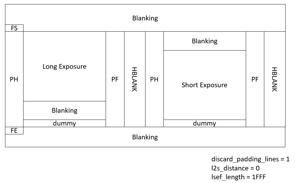
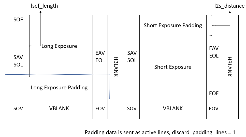
When the manual WDR mode is turned on, MIPI-Rx will allocate the received data to the long exposure frame and short exposure frame according to the following rules.
l2s_distance: The data from the first line to the l2s_distance line are long exposure data, and the long exposure and short exposure are staggered from the l2s_distance+1 line.
lsef_length: Line lsef_length+1 starts with short exposure frame data. Until the next vertical synchronization signal.
When discard_padding_lines=1,the line assignment method from 1 to l2s_distance is {long- ignore -long -ignore }The allocation method from l2s_distance+1 to lsef_length is {long -short -long -short }。 Line lsef_length+1 to the next vertical synchronization signal distribution mode is {short -ignore- short- ignore }.
When discard_padding_lines=0, the allocation method from 1 to l2s_distance is {long -long-long }The allocation method from 2s_distance+1 to sef_length is {long -short- long -short }. Line lsef_length+1 to the next vertical synchronization signal allocation mode is {short- short - short}。
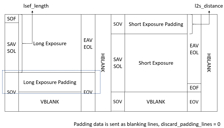
MIPI-Rx must ensure that the number of rows of long exposure frame and short exposure frame sent to ISP is consistent.
Adjust the short exposure length of sensor. It is possible that l2s_distance needs to be adjusted together.
Some sensors may bring dummy line after sending effective data of short exposure. This will cause the number of rows of long exposure and short exposure to be inconsistent. You can set l2s_distance to 0, lsef_length to the maximum value of 0x1fff, discard_padding_lines to 1, that is, you can receive two long and short exposures with valid and dummy data, and then use ISP crop to locate them.