2. MIPI DSI
Overview
The Display Serial Interface (DSI) is a high-speed serial interface defined by Mobile Industry Processor Interface alliance(MIPI Alliance), which is mainly used for the connection between processor and display module.
This document describes how to develop and debug MIPI LCD screen on CVITEK processor solution to help customers develop MIPI LCD business orderly and quickly.
2.1. Environment preparation
2.1.1. Introduction of MIPI DSI screen interface
MIPI DSI screen generally has the following signals, as shown in the figure.
MIPI clock(CLK)
MIPI data(DATA), can be up to 4Lane(can only be 1/2/4Lane)
Backlight control signal(BACKLIGHT)
Reset pin (RESET)
Screen power supply(POWER)
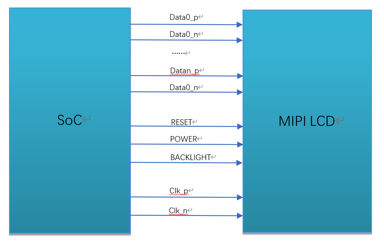
Fig. 2.1 Connection diagram of MIPI DSI interface
2.1.2. Hardware Connection Confirmation
Check the hardware connection and make sure there is no abnormal condition. Some specific pin differences need to be confirmed by referring to the specifications and circuit schematic provided by the screen manufacturer.
2.2. Configure MIPI Screen
According to the content of environment preparation in the previous section, the configuration of screen porting is understood in the interface and connection. In this chapter, software configuration is described when the screen is porting.
CVITEK has two methods for MIPI screen docking, which are screen initialized in u-boot and kernel respectively. The difference is that after initialization in u-boot, the user’s logo image can be displayed after booting, while products with screen basically have the need to display logo. In practical application, choose one of the two according to the demand.
2.2.1. Configuring MIPI Screen in u-boot
The MIPI screen is configured in u-boot by the command showlogo developed by CVITEK. After the device is powered on, press Enter to enter the u-boot command line interface, the command showlogo(it might be different per boards) can be seen after the command printenv is excuted, bootcmd will execute the command to initialize the screen and display the logo before booting the kernel.
Example:
showlogo=mmc dev 0;mmc read 0x84080000 0xA000 0x400; cvi_jpeg 0x84080000 0x81800000 0x80000; startvo 0 8192 0;startvl 0 0x84080000 0x81800000 0x80000 32;setvobg 0 0xffffffff
This document focuses on the initialization part of the screen, and for details of logo display, please refer to 《CVITEK Startup Screen User Guide》. The initialization part of the screen is implemented in “startvo 0 81920”.
2.2.1.1. Configuring MIPI Tx Device Properties
According to the screen specification, the configuration header file of each screen is implemented and placed in the path
u-boot-2021.10/include/cvitek/cvi_panels/, customers can add their own screen header files by referring to other header file templates.
combo_dev_cfg_s structure definition
struct combo_dev_cfg_s {

   unsigned int devno;

   enum mipi_tx_lane_id lane_id[LANE_MAX_NUM];

   enum output_mode_e output_mode;

   enum video_mode_e video_mode;

   enum output_format_e output_format;

   struct sync_info_s sync_info;

   unsigned int pixel_clk;

   bool lane_pn_swap[LANE_MAX_NUM];

};
Member name |
Description |
|---|---|
devno |
MIPI Tx device number,default to 0 |
lane_id |
The corresponding relationship between the lane numbers of the host controller and the screen , fill in -1 for the unused lane. There are 5 lanes in total, which represent MIPI_TX_0~MIPI_TX_4 of the host controller in sequence. The actual content should be filled in according to the MIPI screen number corresponding to the screen. For example, if the first member is MIPI_TX_0 of the host controller, check the circuit schematic and fill in MIPI_TX_LANE_3 according to the corresponding MIPI lane3 in screen. An incorrect corresponding relationship will not light up the screen. |
output_mode |
MIPI Tx output mode,default to OUTPUT_MODE_DSI_VIDEO |
video_mode |
MIPI Tx video mode,default to BURST_MODE |
output_format |
MIPI Tx output format,default to OUT_FORMAT_RGB_24_BIT |
sync_info |
Synchronization information of MIPI Tx device |
pixel_clk |
Pixel clock (unit: KHz). Calculation formula: pixel_clk=(htotal*vtotal)*fps/1000 In which: htotal=vid_hsa_pixels+ vid_hbp_pixels+ vid_hfp_pixels+ vid_hline_pixels vtotal= vid_vsa_lines+ vid_vbp_lines+ vid_vfp_lines+ vid_active_lines fps: frame rate,default to 60 .Deducing lane_clk from pixel_clk, we can get the transform equation: lane_clk= pixel_clk*24/4/2(24 means that each pixel of RGB888 takes up 24bits, 4 means that 4 data lanes are used, and 2 means that MIPI_CLK is triggered by double edge) |
lane_pn_swap |
Whether Lane P/N pole of MIPI Tx swaps true:swap false: no swapping |
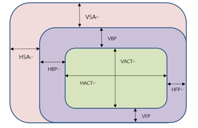
sync_info(synchronization information of MIPI Tx device) in combo_dev_cfg_s is difficult to configure. The configuration method is described in detail below. Generally, the reference values will be filled in according to the specifications provided by the screen manufacturer, and the further problems should be adjusted according to the phenomenon.
sync_info_s structure definition
struct sync_info_s {

   unsigned short vid_hsa_pixels;

   unsigned short vid_hbp_pixels;

   unsigned short vid_hfp_pixels;

   unsigned short vid_hline_pixels;

   unsigned short vid_vsa_lines;

   unsigned short vid_vbp_lines;

   unsigned short vid_vfp_lines;

   unsigned short vid_active_lines;

   bool vid_vsa_pos_polarity;

   bool vid_hsa_pos_polarity;

};
Member name |
Description |
|---|---|
vid_hsa_pixels |
horizontal sync active(HSA). Unit: pixel |
vid_hbp_pixels |
horizontal back porch(HBP). Unit: pixel |
vid_hfp_pixels |
Horizon front porch(HFP). Unit: pixel |
vid_hline_pixels |
Horizontal active region(HACT). Unit: pixel |
vid_vsa_lines |
Vertical Sync Active(VSA). Unit: line |
vid_vbp_lines |
Vertical Back Porch (VBP). Unit: line |
vid_vfp_lines |
Vertical front porch(VFP). Unit: line |
vid_active_lines |
Vertical Active region(VACT). Unit: line |
vid_vsa_pos_polarity |
Polarity of vertical active signal, with 0 as high effective and 1 as low effective |
vid_hsa_pos_polarity |
Polarity of horizontal active signal, with 0 as high effective and 1 as low effective |
Sketch map of MIPI pixel area under MIPI DSI protocol
hs_settle_s structure definition
struct hs_settle_s {

  unsigned char prepare;

  unsigned char zero;

  unsigned char trail;

};
Member Name |
Description |
|---|---|
prepare |
MIPI Tx prepare signal,default value: 6 |
zero |
MIPI Tx zero signal,default value: 32 |
trail |
MIPI Tx trail signal,default value: 1 |
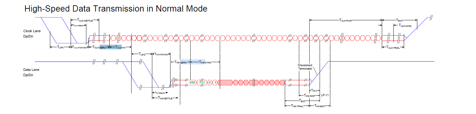
Fig. 2.2 MIPI Tx Sequence Diagram
Example:
const struct combo_dev_cfg_s dev_cfg = {
   .devno = 0,
   .lane_id = {MIPI_TX_LANE_3, MIPI_TX_LANE_0, MIPI_TX_LANE_CLK, MIPI_TX_LANE_2, MIPI_TX_LANE_1},
   .lane_pn_swap = {false, false, false, false, false},
   .output_mode = OUTPUT_MODE_DSI_VIDEO,
   .video_mode = BURST_MODE,
   .output_format = OUT_FORMAT_RGB_24_BIT,
   .sync_info = {
      .vid_hsa_pixels = 30,
      .vid_hbp_pixels = 100,
      .vid_hfp_pixels = 100,
      .vid_hline_pixels = 800,
      .vid_vsa_lines = 4,
      .vid_vbp_lines = 16,
      .vid_vfp_lines = 10,
      .vid_active_lines = 1280,
      .vid_vsa_pos_polarity = false,
      .vid_hsa_pos_polarity = true,
   },
   .pixel_clk = 80958,
};

const struct hs_settle_s hs_timing_cfg = { .prepare = 6, .zero = 32, .trail = 1 };
2.2.1.2. Configuring Screen Initialization Sequence
The screen generally has initialization process. MIPI LCD screen sends the specified type of data package through MIPI Tx D-PHY interface. Initialization sequence is provided by the screen manufacturer.
The initialization sequence of the screen generally includes pixel format, direction of data refreshing, Gamma configuration, etc. The specific meaning of each instruction in the initialization sequence can be found in the specification by the screen manufacturer provided or Driver IC Datasheet. Initialization sequence is sent through Data Lane0 in LP mode of MIPI Tx, and will switch to HS mode afterwards.
dsc_instr structure definition
struct dsc_instr {

  u8 delay;

  u8 data_type;

  u8 size;

  u8 data[0x60];

};
The initialization sequence provided by the screen manufacturer generally includes register address and corresponding data. According to the sequence provided by the screen manufacturer, the data type, data address and data should be filled.
Member Name |
Description |
|---|---|
delay |
The milliseconds of delay after sending this command |
data_type |
Write command data type, that is, the Data Type in DCS (DisplayCommandSet). Select the data type according to the number of data. Type 1. When there is only the register address and no data, the data type is 0x05; Type 2: when there are a register address and a data, the data type is as 0x15 or 0x23; Type 3: when there are register addresses and the number of data is greater than or equal to 2. Generally, the data type is 0x29 or 0x39. It is common in general, please consult the screen manufacturer for the specific usage. |
size |
The sum of register address and data number. For example, if there is only one register address, fill in 1; When there are one register address and one data, fill in 2; one register address and two data, fill in 3, and so on. |
data |
Pointer of command and data. Register address and data. The first one must be the register address, followed by the data, which can be absent or multiple. |
Note: consult the manufacturer for the configuration of parameters of command data type. If it is not supported by the manufacturer, it is recommended to fill in 0x05 when there is no data, 0x15 when there is one data, and 0x29 when there are multiple data.
Example:
static u8 data_xxxx_0[] = { 0xFF, 0x98, 0x81, 0x03 };

static u8 data_xxxx_1[] = { 0x01, 0x00 };

static u8 data_xxxx_2[] = {0x02, 0x00 };

......

static u8 data_xxxx_n[] = { 0x11 };

static u8 data_xxxx_n+1[] = { 0x29 };

const struct dsc_instr dsi_init_cmds[] = {

{ .delay = 0, .data_type = 0x29, .size = 4, .data = data_xxxx_0 },

{ .delay = 0, .data_type = 0x15, .size = 2, .data = data_xxxx_1 },

{ .delay = 0, .data_type = 0x15, .size = 2, .data = data_xxxx_2 },

......

{ .delay = 120, .data_type = 0x05, .size = 1, .data = data_xxxx_n },

{ .delay = 20, .data_type = 0x05, .size = 1, .data = data_xxxx_n+1 },

}
2.2.1.3. Adding Reference to the Header File
Add a reference to the newly added and header file which is mentioned in the previous two sections in u-boot-2021.10/include/cvitek/cvi_panels/cvi_panels.h.
Example:
#ifdef MIPI_SCREEN_HX8394
#include "dsi_hx8394_evb.h"
static struct screen_desc_s screen_desc = {
     .screen_name = "HX8394-720x1280",
     .dev_cfg = &dev_cfg_hx8394_720x1280,
     .hs_timing_cfg = &hs_timing_cfg_hx8394_720x1280,
     .dsi_init_cmds = dsi_init_cmds_hx8394_720x1280,
     .dsi_init_cmds_size = ARRAY_SIZE(dsi_init_cmds_hx8394_720x1280)
};
#endif
2.2.1.4. Configuring RESET pin of MIPI Screen
Add the control of RESET/POWER/BACKLIGHT in function mipi_tx_set_combo_dev_cfg of u-boot-2021.10/drivers/video/cvitek/cvi_mipi.c.
Generally RESET pin of MIPI screen uses the GPIO port. So we need to configure the GPIO port and then reset the screen.
Check the circuit schematic to get the pin name corresponding to the RESET pin.
Find the GPIO group number and serial number corresponding to the pin according to《CV181x_PINOUT_CN》.
Revise the reset in vo node in 改build/default/dts/cv181x/cv181x_base.dtsi to the corresponding value.
Configure the reset operation sequence of GPIO for RESET.
The reset operation of the screen needs to refer to the screen specification. If there is no reset operation, or the reset timing does not match the requirements of the screen, or the level does not match, the screen may not light up or work abnormally. Generally speaking, it is a high-low-high level change. Please refer to the screen specification for details.
Example:Suppose the RESET pin of the screen is GPIOE 2, the reset voltage is low. The revision in 改build/default/dts/cv181x/cv181x_base.dtsi is as follow:
reset-gpio = <&porte 2 GPIO_ACTIVE_LOW>;
The configurations are as follow:
gpio_request_by_name(dev, "reset-gpio", 0, &priv->ctrl_gpios.disp_reset_gpio, GPIOD_IS_OUT | GPIOD_IS_OUT_ACTIVE);
the operations are as follow:
dm_gpio_set_value(&ctrl_gpios.disp_reset_gpio, ctrl_gpios.disp_reset_gpio.flags & GPIOD_ACTIVE_LOW ? 0 : 1);
mdelay(10);
dm_gpio_set_value(&ctrl_gpios.disp_reset_gpio, ctrl_gpios.disp_reset_gpio.flags & GPIOD_ACTIVE_LOW ? 1 : 0);
mdelay(10);
dm_gpio_set_value(&ctrl_gpios.disp_reset_gpio, ctrl_gpios.disp_reset_gpio.flags & GPIOD_ACTIVE_LOW ? 0 : 1);
mdelay(100);
The RESET pin will perform a high-low-high level change after these steps.
2.2.1.5. Configuring MIPI Screen POWER pin
Generally, GPIO function is also used for POWER pin of MIPI screen. The power supply status of MIPI screen usually can be controlled by pulling up or down the pin level. Some screens may be powered directly so that there is no need to control in software.
Configuration is consistent with the RESET pin mentioned in the previous section
Example:
Suppose that the POWER control pin of the screen is GPIOE 0. The revision in build/default/dts/cv181x/cv181x_base.dtsi is as follow:
power-ct-gpio = <&porte 0 GPIO_ACTIVE_HIGH>;
The POWER can be delete directly if there is no need to configure.
The configurations are as follow:
gpio_request_by_name(dev, "power-ct-gpio", 0, &priv->ctrl_gpios.disp_power_ct_gpio, GPIOD_IS_OUT | GPIOD_IS_OUT_ACTIVE);
the operation is as follow:
dm_gpio_set_value(&ctrl_gpios.disp_power_ct_gpio, ctrl_gpios.disp_power_ct_gpio.flags & GPIOD_ACTIVE_LOW ? 0 : 1);
2.2.1.6. Configure MIPI Screen BACKLIGHT pin
The BACKLIGHT of MIPI screen can be configured to GPIO or PWM.
2.2.1.6.1. Configure as GPIO
The configuration metheod is consistent with the configuration method of RESRT pin mentioned in the lat section.
Example:
Suppose the PWM pin of the screen is GPIOE 1 and the working voltage is high. The revision in build/default/dts/cv181x/cv181x_base.dtsi is as follow:
pwm-gpio = <&porte 1 GPIO_ACTIVE_HIGH>;
The POWER can be delete directly if there is no need to configure.
The configurations are as follow:
gpio_request_by_name(dev, "pwm-gpio", 0, &priv->ctrl_gpios. disp_pwm_gpio, GPIOD_IS_OUT | GPIOD_IS_OUT_ACTIVE);
the operation is as follow:
dm_gpio_set_value(&ctrl_gpios.disp_pwm_gpio, ctrl_gpios.disp_pwm_gpio.flags & GPIOD_ACTIVE_LOW ? 0 : 1);
2.2.1.6.2. Configure as PWM
Generally, the BACKLIGHT of MIPI screen can adjust brightness via PWM.
Check the circuit schematic to get the pin name corresponding to the BACKLIGHT pin.
In function “board_init” of u-boot-2021.10/board/cvitek/cv181x/board.c configure the multiplexing function of BACKLIGHT pin as PWM function.
According to the register information in the chapter of peripheral PWM in《CV181x Preliminary Datasheet》, configure the periods, duty cycle and enable of PWM.
Base address of PWM is as follows, refer to 《CV181x Preliminary Datasheet》 for other register information. CV181x has 4 groups of PWM with 4 channels in each group.
PWM0 |
0x03060000 |
PWM1 |
0x03061000 |
PWM2 |
0x03062000 |
PWM3 |
0x03063000 |
Note: PWM0~3 here is the PWM group number, while the circuit schematic or pinlist shows PWM0~PWM15. If you see PWM1, it corresponds to PWM0_1, the first channel of group 0 in the above table.
Example:
Suppose BACKLIGHT pin of the screen is PWM1,
_reg_write(0x03060008, 0x3E8);// ()PWM1 low-level counts (unit: NS)
_reg_write(0x0306000C, 0xF4240);// Periodic count number of PWM1 square wave(unit: ns)
_reg_write(0x03060044, 0x02);// Enable PWM output
2.2.1.7. Configuring u-boot Environment Variables
Modify the parameters of u-boot environment variables in u-boot-2021.10/include/configs/cv181x-asic.h
Example:
define SHOWLOGOCMD LOAD_LOGO CVI_JPEG START_VO START_VL SET_VO_BG
LOAD_LOGO reads the picture from the MISC partition to the DRAM, CVI_JPEG parses the picture to the specified position, START_VO and START_VL turn on the VO and display the logo in the center position, SET_VO_BG sets the VO background color, and other areas of the screen except logo are filled with this color.
2.2.1.8. Changing Logo Image
Place the customer’s logo image in the path build/tools/common/bootlogo/, and executing build_all will copy the logo to image generation path.
Note: The I80 screen needs 24bit BMP pictures and the rest needs YUV420 format jpg.
2.2.1.9. Compiling and Burning Verification
After the steps above are completed, recompile and burn the new u-boot. Power on, press Enter to enter the u-boot command line interface. Excute the command run showlogo, and you can see the logo image on the screen if the process goes well. If the logo is not displayed, please confirm the following steps.
Make sure the backlight is on.
Make sure the RESET pin level has reached the expected level.
Confirm that the power supply of the screen is normal.
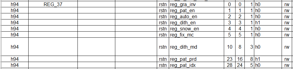
Execute mw 0x0a088094 0x0701000a and output the test pattern of VO. If the screen is initialized successfully, you will see the colorbar.
The figure below shows the test pattern register

If any of the exceptions above are found, please go back to check whether the previous process is set correctly and meets the expectation.
If no abnormality is found in the above, it is recommended to check the Driver IC datasheet or directly consult the screen manufacturer how to turn on the screen BIST mode, usually it is to adjust the register value in the initialization sequence, and the colorbar will be displayed.
If the BIST mode is abnormal, you need to check whether the MIPI Lane sequence, RESET, POWER, PWM, etc. are configured correctly, and use the multimeter / oscilloscope to confirm that the circuit level status meets the expectation. If all meet the expectation, the problem may be the screen itself, please consult the screen manufacturer.
If BIST is normal, it means that the configuration above is correct and the hardware circuit is normal. In this case, it is usually necessary to adjust parameters in sync_info_s.
2.2.2. Configuring MIPI Screen in Kernel
The method of configuring MIPI screen in kernel is almost the same as that in u-boot, but the implementation process is different. You can choose this method when you don’t need to display the logo.
In addition, you can also use kernel mode to debug first, and then port to u-boot to avoid burning u-boot frequently.
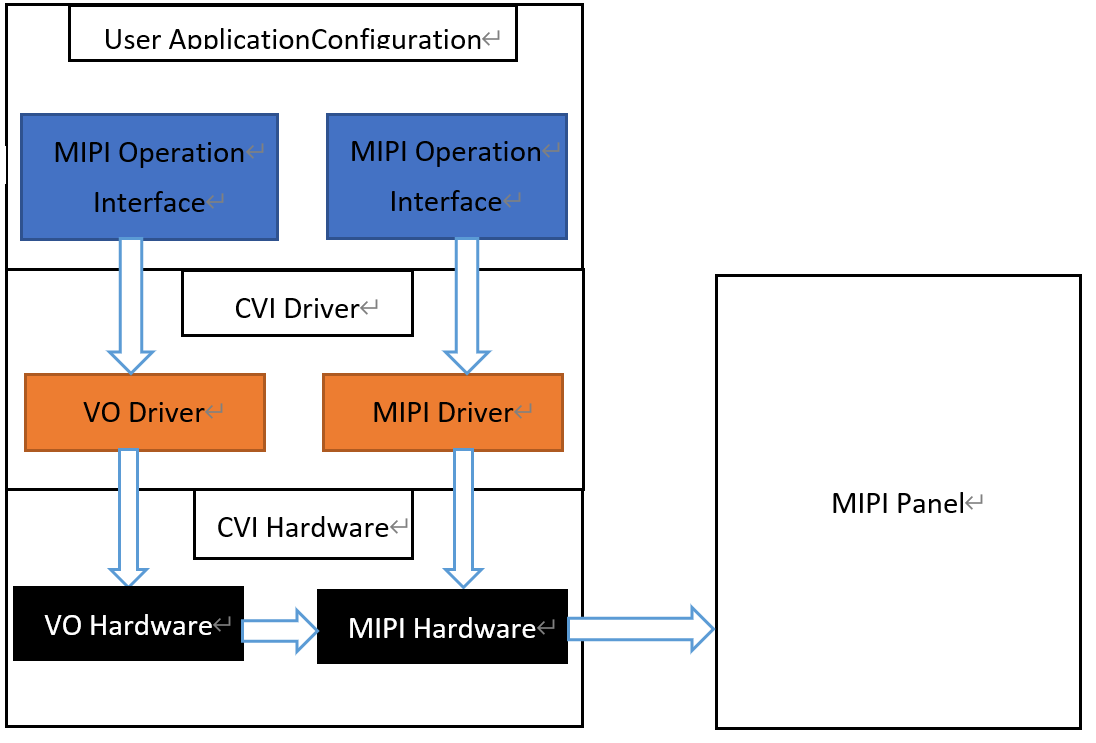
Fig. 2.3 Basic block diagram of docking MIPI screen in kernel
2.2.2.1. Configuring MIPI Tx Device Properties
According to the screen specification, the configuration header file of each screen is implemented and placed in the path middleware/v2/component/panel/cv181x/. Customers can add their own screen header file by referring to other header file templates.
Please refer to section 2.2.1.1
2.2.2.2. Configuring Screen Initialization Sequence
Refer to section 2.2.1.2
2.2.2.3. Add a Reference to the Header File
Add a reference to the newly added header file. Add a reference to the newly added header file mentioned in the previous two sections in middleware/v2/sample/sample_panel/sample_panel.c.
Example:
To light up the screen HX8394_EVB, first include the header file dsi_hx8394_evb.h of the screen in middleware/v2/sample/sample_panel/sample_panel.c, and then ensure that the character array static char *s_panel_model_type_arr[ ] in the middleware/v2/sample/sample_panel/sample_panel.c file contains the character “HX8394_EVB”. If not, add it yourself. Next, add an enumerator HX8394_EVB that is equal to the character index value in the file screen enumeration type PANEL_MODEL. Finally, add a case to call the screen related parameters in the SAMPLE_SET_PANEL_DESC function, as shown below:
case DSI_PANEL_HX8394_EVB:
        g_panel_desc.panel_type = PANEL_MODE_DSI;
        g_panel_desc.stdsicfg.dev_cfg = &dev_cfg_hx8394_720x1280;
        g_panel_desc.stdsicfg.hs_timing_cfg = &hs_timing_cfg_hx8394_720x1280;
        g_panel_desc.stdsicfg.dsi_init_cmds = dsi_init_cmds_hx8394_720x1280;
        g_panel_desc.stdsicfg.dsi_init_cmds_size = ARRAY_SIZE(dsi_init_cmds_hx8394_720x1280);
        break;
2.2.2.4. Configuring MIPI Screen RESET, POWER, BACKLIGHT pins
Method 1:
Find the corresponding DTS file in path build/boards/default/dts/cv181x/ and configure the GPIO information of MIPI TX. If there is no such pin, you can skip it directly.
Example:
mipi_tx: mipi_tx {
        compatible = "cvitek,mipi_tx";
        reset-gpio = <&porte 2 GPIO_ACTIVE_LOW>;
        pwm-gpio = <&porte 0 GPIO_ACTIVE_HIGH>;
        power-ct-gpio = <&porte 1 GPIO_ACTIVE_HIGH>;
        clocks = <&clk CV181X_CLK_DISP_VIP>, <&clk CV181X_CLK_DSI_MAC_VIP>;
        clock-names = "clk_disp", "clk_dsi";
};
Instruction:
pwm-gpio = <&portb 0 GPIO_ACTIVE_HIGH>;
For the convenience of debugging, you can use GPIO function to control the backlight first, and remember not to configure function of pinmux as PWM in u-boot, otherwise you may not be able to control it.
Later, if you have to adjust the brightness for your needs, you can then configure the function of pinmux as PWM in u-boot, delete this PWM configuration in dts, and control it in app by using PWM.
After the system is booted, the method of loading MIPI Tx driver (Usually it will be automatically loaded, you can first use lsmod to check if it has been loaded):
insmod /mnt/system/ko/cvi_mipi_tx.ko
In this way, when the driver is loaded, it will automatically apply for these GPIO resources according to the GPIO information in dts and initialize them to the corresponding level state.
Method 2:
There is no need to modify the kernel dts file.
After the system is booted, the method of loading MIPI Tx driver:
insmod /mnt/system/ko/cvi_mipi_tx.ko gpio=424,0,425,1,452,1
The three GPIOs are RESET, POWER and PWM in sequence.
When the driver is loaded, the driver will automatically apply for the GPIO resources corresponding to the GPIO numbers by using the information in the gpio parameters preferentially, and initialize to the subsequent level state. If there is no GPIO parameter, the driver will apply for GPIO resources according to the GPIO information in dts. If there is no such pin, the GPIO number and level status can be written to -1.
Similarly, for the convenience of debugging, the backlight can be controlled by GPIO function first, and function of pinmux should not be configured as PWM in u-boot. Later, if we need to adjust the brightness, we need configure the function of pinmux as PWM in u-boot. At the same time, we control it in app by using PWM, and write the third GPIO number and level state as -1.
Method 3:
Control these GPIOs in user space directly.
Example: Assuming reset: GPIOB5, pwm: GPIOB3, power: GPIOB4, You can use the cat /sys/kernel/debug/gpio command to view the GPIO configuration of the chip, and obtain the numbering range from gpiochip0 to gpiochip4, corresponding to the numbering range from GPIOA to GPIOB. If the range of gpiochip1 is 448 to 479, then for the GPIOB5 to be pulled, the number of the echo operation below can be obtained from 448+5=453.
Therefore, the following operations are required to pull the corresponding pins:
1. echo 453 > /sys/class/gpio/export
   echo 451 > /sys/class/gpio/export
   echo 452 > /sys/class/gpio/export
2. echo out > /sys/class/gpio/gpio453/direction
   echo out > /sys/class/gpio/gpio451/direction
   echo out > /sys/class/gpio/gpio452/direction
3. echo 1 > /sys/class/gpio/gpio453/value
   echo 1 > /sys/class/gpio/gpio451/value
   echo 1 > /sys/class/gpio/gpio452/value
   echo 0 > /sys/class/gpio/gpio453/value
   echo 1 > /sys/class/gpio/gpio453/value
Instruction:
For the convenience of debugging, you can use GPIO function to control the backlight first, and remember not to configure function of pinmux as PWM in u-boot, otherwise you may not be able to control it.
Later, if you have to adjust the brightness for your needs, you can then configure the function of pinmux as PWM in u-boot, and control it in app by using PWM.
2.2.2.5. Compiling and Verificating
Execute build_middleware to compile middleware, and executable file sample_panel will be generated in the path middleware/v2/sample/sample_panel/. The program does the same thing as what “startvo 0 65536 0” does in u-boot. It switches to LP mode, sets MIPI Tx device properties, sends initialization sequence to screen through Data Lane0, and then switches back to HS mode.
Copy sample_panel to device , and after executing the command ./sample_panel, it will prompt the execution method of the command. Follow the prompts to run.
Description:
If the initial level of RESET pin is set to low, a high-low-high timing change is needed.
If the initial level of RESET pin is set to high, a low-high-low timing change is needed.
Enable VO test pattern, register is as shown in the figure below. You will see the colorbar after executing devmem 0x0a088094 32 0x0701000a.
If the colorbar does not display normally, please check whether the previous process is set correctly and meets the expectation.
If no abnormality is found in the previous process, it is recommended to check the Driver IC datasheet or directly consult the screen manufacturer about how to open the BIST mode of the screen. Usually, it is to adjust a register value in the initialization sequence, and colorbar will be displayed.
If the BIST mode is abnormal, you need to check whether the MIPI Lane sequence, RESET, POWER, PWM, etc. are configured correctly, and use the multimeter/ oscilloscope to confirm that whether the circuit level status meets the expectation. If all meet the expectation, it may be the problem of the screen itself, please consult the screen manufacturer.
If BIST is normal, it means that the configuration above is correct and the hardware circuit is normal. In this case, it is usually necessary to adjust sync_info_s.
2.2.3. Configure MIPI Screen in Dual_OS
The method of configuring MIPI screen in Dual_OS is almost the same as in the single system mentioned above, with some minor differences. Below are the similarities and differences.
Docking MIPI Screen Basic Block Diagram
Among them, the VO and MIPI drivers in the above figure are both completed in the small kernel alios.
2.2.3.1. Configuring MIPI Tx Device Properties
Configure MIPI Tx device properties according to the screen specifications, implement configuration header files for each screen, and place them in the paths middleware/v2/component/panel/cv181x/ and cvi_alios/components/cvi_mmf_sdk/cvi_mddleware/include/panel/. Customers can refer to other header file templates to add their own panel header files.
Refer to section 2.2.1.1
2.2.3.2. Configuring Screen Initialization Sequence
Refer to section 2.2.1.2.
2.2.3.3. Turn on the configuration switch in cvi_alios
Turn on the switches for the corresponding chip and screen type in cvi_alios/solutions/normboot/package_yamls/package.yaml.turnkey.
For example, if the CONFIG_BOARD_CV181XH chip is selected and the CONFIG_PANEL_HX8394 screen is displayed, the following switch will be turned on:
CONFIG_BOARD_CV181XC: 0
CONFIG_BOARD_CV181XH: 1

CONFIG_PANEL_HX8394: 1
Note that if the CONFIG_BOARD_CV181XC chip needs to support both sensors and panels, hardware modification is required, and pin multiplexing in the _MapiTxPinmux() interface in cvi_ilios/solutions/normboot/customization/cv1811c_cv2003_1l_triple/src/customer_platform.c needs to be modified as needed.
2.2.3.4. Add a Reference to the Header File
Refer to section 2.2.2.3.
2.2.3.5. Configuring MIPI Screen RESET, POWER, BACKLIGHT pins
Add multiplexing of RESET, POWER, and BackLIGHT pins in the _MipiTxPinmux interface of cvi_ios/solutions/normboot/customization/cv1811c_cv2003_1l-triple/src/customer_platform.c, and then directly control GPIO at the application layer.
Example:
For the PROFIG-BOARD-CV181XH chip, the general pin to be pulled is: reset: GPIOE2, pwm:GPIOE0,power:GPIOE1。
Therefore, the following operations are required to pull the corresponding pins:
devmem 0x03022004 32 0x0
devmem 0x03022000 32 0x0
echo 352 > /sys/class/gpio/export
echo 353 > /sys/class/gpio/export
echo 354 > /sys/class/gpio/export
echo out > /sys/class/gpio/gpio352/direction
echo out > /sys/class/gpio/gpio353/direction
echo out > /sys/class/gpio/gpio354/direction
echo 1 > /sys/class/gpio/gpio354/value
echo 1 > /sys/class/gpio/gpio352/value
echo 1 > /sys/class/gpio/gpio353/value
For the PROFIG-BOARD-CV181XC chip, the general pin to be pulled is: reset: GPIOA15, pwm:GPIOA18,power:GPIOA19。
Therefore, the following operations are required to pull the corresponding pins:
devmem 0x0300103c 32 0x3
devmem 0x03001068 32 0x3
devmem 0x03001064 32 0x3
echo 495 > /sys/class/gpio/export
echo 498 > /sys/class/gpio/export
echo 499 > /sys/class/gpio/export
echo out > /sys/class/gpio/gpio495/direction
echo out > /sys/class/gpio/gpio498/direction
echo out > /sys/class/gpio/gpio499/direction
echo 1 > /sys/class/gpio/gpio495/value
echo 1 > /sys/class/gpio/gpio498/value
echo 1 > /sys/class/gpio/gpio499/value
echo 0 > /sys/class/gpio/gpio495/value
echo 1 > /sys/class/gpio/gpio495/value
The devmem register writing instruction in the above code is to reuse the corresponding pins. If the relevant multiplexing has been completed, this instruction may not be executed.
2.2.3.6. Compiling and Verificating
Refer to section 2.2.2.5.