3. LVDS
Overview
Low Voltage Differential Signal (LVDS) is a type of video signal transmission mode developed by National Semiconductor Corporation (NS) in 1994 to overcome the disadvantages of high power consumption and electromagnetic interference (EMI) in transmitting high-bit-rate data using TTL voltage levels. LVDS interface, also known as RS644 bus interface, is an electrical standard widely used in LCD screen interfaces. The overall LVDS screen is similar to MIPI, but there are some differences. This section introduces how to develop and debug LVDS LCD screens on the CVITEK processor solution.
3.1. Environment Preparation
3.1.1. LVDS Screen Docking Instruction
LVDS screen generally has the following signals, as shown in the figure:
LVDS clock(CLK)
LVDS data(DATA)(single-ended 6bit:3 lane, single-ended 8bit:4 lane,single-ended 10bit:5 lane,double-ended 6bit:6 lane,double-ended 6bit:8 lane,double-ended 6bit:10 lane,Now it only supports single-ended 6bit and single-ended 8bit)
Backlight control signal(BACKLIGHT)
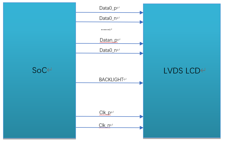
Fig. 3.1 Connection diagram of LVDS interface
3.1.2. Hardware Connection Confirmation
Check the hardware connection and make sure there is no abnormal condition. Some specific pin differences need to be confirmed by referring to the specifications and circuit schematic provided by the panel manufacturer.
3.2. Configure LVDS Screen
Based on the content of the previous section on environmental preparation, the configuration of the screen interface and wiring has been understood. In this section, we will explain the software configuration required for screen interface.
CVITEK has two solutions for LVDS screen interface, similar to MIPI screens, which are initialized in u-boot and kernel respectively. In actual applications, either one can be chosen according to the requirements.
3.2.1. Configure LVDS Screen in u-boot
To configure a MIPI screen in u-boot, the CVITEK-developed ‘showlogo’ command is used. After the device is powered on, enter the u-boot command line by pressing enter, and the ‘printenv’ command can display the ‘showlogo’ command. The ‘bootcmd’ command will execute this command to initialize and display the screen logo before booting the kernel.
Example:
showlogo=mmc dev 0;mmc read 0x84080000 0xA000 0x400; cvi_jpeg 0x84080000 0x81800000 0x80000; startvo 0 2048 0;startvl 0 0x84080000 0x81800000 0x80000 16;setvobg 0 0xffffffff
Note: Single-ended 6-bit is 1024, single-ended 8-bit is 2048, and single-ended 10-bit is 4096.
This document focuses on the initialization part of the screen, and for displaying the logo, please refer to the 《CVITEK Startup Screen User Guide》. The initialization part of the screen is implemented in ‘startvo 0 2048 0’.
3.2.1.1. Configure LVDS Device Properties
According to the screen specification, the configuration header file of each screen is implemented and placed in the path
u-boot-2021.10/include/cvitek/cvi_panels/, customers can add their own panel header files by referring to other header file templates.
cvi_lvds_cfg_s structure definition
struct cvi_lvds_cfg_s {
    enum LVDS_OUT_BIT       out_bits;
    enum LVDS_MODE          mode;
    unsigned char           chn_num;
    bool                    data_big_endian;
    enum lvds_lane_id       lane_id[LANE_MAX_NUM];
    bool                    lane_pn_swap[LANE_MAX_NUM];
    struct sync_info_s      sync_info;
    unsigned short          u16FrameRate;
    unsigned int            pixelclock;
};
Member name |
description |
|---|---|
out_bits |
LVDS_OUT_6BIT、LVDS_OUT_8BIT、LVDS_OUT_10BIT |
mode |
LVDS_MODE_JEIDA、LVDS_MODE_VESA,it’s usually set to LVDS_MODE_VESA |
chn_num |
Channel number 1、2,now the processor only supports channel number 1 |
data_big_endian |
The byte order for sending data,it’s usually set to false |
Lane_id |
The correspondence between the Lane numbers of the host and the screen end, with unused Lanes filled in with -1. There are a total of 5 members, representing the VO_LVDS_LANE_0 ~ VO_LVDS_LANE_4 of the host sequentially, and the actual content needs to be filled in according to the LVDS Lane numbers corresponding to the screen end. For example, if the first member is Host Lane 0, according to the circuit schematic, it corresponds to Screen Lane 3, and thus VO_LVDS_LANE_3 should be filled in. Incorrect correspondence will result in the screen not lighting up. |
lane_pn_swap |
Whether the Lane P/N poles of LVDS are exchanged true:exchange false:don’t exchange |
sync_info |
The synchronization information of LVDS devices |
pixel_clk |
Pixel clock (unit: KHz). Calculation formula: pixel_clk=(htotal*vtotal)*fps/1000 In which: htotal=vid_hsa_pixels+ vid_hbp_pixels+ vid_hfp_pixels+ vid_hline_pixels vtotal= vid_vsa_lines+ vid_vbp_lines+ vid_vfp_lines+ vid_active_lines fps: frame rate,default to 60 Deducing lane_clk from pixel_clk, we can get transform equation: lane_clk= pixel_clk*24/4/2(24 means that each pixel of RGB888 (each pixel consists of three channels which take up 8 bit respectively) takes up 24bits, 4 means that 4 data lanes are used, and 2 means that MIPI_CLK is triggered by double edge) |
example:
struct cvi_lvds_cfg_s lvds_ek79202_cfg = {
    .mode = LVDS_MODE_VESA,
    .out_bits = LVDS_OUT_8BIT,
    .chn_num = 1,
    .lane_id = {VO_LVDS_LANE_0, VO_LVDS_LANE_1, VO_LVDS_LANE_2, VO_LVDS_LANE_3, VO_LVDS_LANE_CLK},
    .lane_pn_swap = {false, false, false, false, false},
    .sync_info = {
       .vid_hsa_pixels = 10,
       .vid_hbp_pixels = 88,
       .vid_hfp_pixels = 62,
       .vid_hline_pixels = 1280,
       .vid_vsa_lines = 4,
       .vid_vbp_lines = 23,
       .vid_vfp_lines = 11,
       .vid_active_lines = 800,
       .vid_vsa_pos_polarity = 0,
       .vid_hsa_pos_polarity = 0,
    },
    .u16FrameRate = 60,
    .pixelclock = 72403,
};
sync_info_s structure definition
Similar to MIPI, please refer to 2.2.1.1.
LVDS Sequence Diagram

3.2.1.2. Adding Reference to the Header File
Add a reference to the newly added header file. In u-boot-2021.10/include/cvitek/cvi_panels/cvi_panels.h, add a reference to the newly added header file in the previous section.
example:
#if defined(LVDS_PANEL_EK79202)
#include "lvds_ek79202.h"
static struct panel_desc_s panel_desc = {
     .lvds_cfg = &lvds_ek79202_cfg
};
#endif
3.2.1.3. Configure the BACKLIGHT pin of LVDS Screen
The BACKLIGHT of LVDS screen can be set to GPIO or PWM.
3.2.1.3.1. Configure as GPIO
It can be realized by modifying VO_GPIO_PWM_PORT、VO_GPIO_PWM_INDEX、VO_GPIO_PWM_ACTIVE in build/boards/cv181x/cv181xxx/u-boot/cvitek.h
3.2.1.3.2. Configure as PWM
Generally through PWM, this can achieve brightness adjustment. The implementation is similar to the MIPI screen, please refer to 2.2.1.6.
3.2.1.4. Configure u-boot Environment Variables
The operation is similar to MIPI screen,please refer to 2.2.1.7.
3.2.1.5. Changing Logo Image
The operation is similar to MIPI screen,please refer to 2.2.1.8.
3.2.1.6. Compiling and Burning Verification
After the steps above are completed, recompile and burn the new u-boot. Power on, press Enter to enter the u-boot command line interface. Excute the command run showlogo, and you can see the logo image on the panel if the process goes well. If the logo is not displayed, please confirm the following steps.
Make sure the backlight is on.
Confirm that the power supply of the panel is normal.
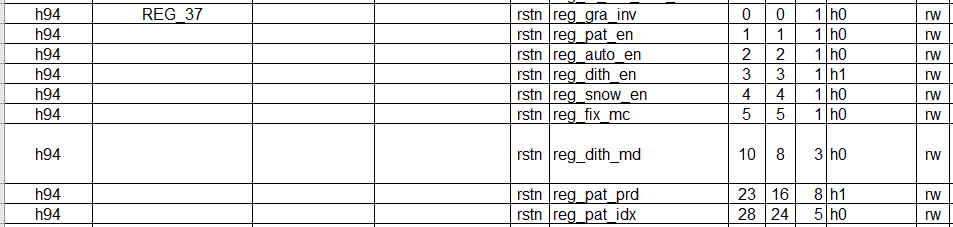
Execute mw 0x0a088094 0x0701000a and output the VO test pattern. If the panel is initialized successfully, you will see the colorbar.
The figure below shows the test pattern register
If any of the exceptions above are found, please go back to check whether the previous process is set correctly and meets the expectation.
If no abnormalities are found in the above steps, it is necessary to further check if the LVDS lane order, PWM, and other configurations are correct, and confirm the circuit voltage status meets the expectations using a multimeter/oscilloscope. If everything is as expected, it may be an issue with the screen itself, and the screen manufacturer should be consulted.
If the configuration and hardware circuit are correct, it is usually necessary to adjust the parameters in sync_info_s.
3.2.2. Configure LVDS in Kernel
The method for configuring LVDS screen in kernel is almost the same as in u-boot, but the implementation process is different. This method can be chosen when there is no need to display the logo. In addition, you can also debug it with the kernel method first, and then transplant it to u-boot to avoid frequent burning of u-boot.
3.2.2.1. Configure LVDS Device Properties
Based on the specification of the screen, implement the configuration header file for each screen and place it in the path middleware/v2/component/panel/cv181x/. Customers can refer to the other header file templates to add their own panel header files.
See section 3.2.1.1 for more details.
3.2.2.2. Add a Reference to the Header File
Add reference to the newly added header file. Add reference to the newly added header file in middleware/v2/sample/sample_panel/sample_panel.c as mentioned in section 3.2.1.1.
example:
To light up the screen LCM185X56, first include the header file lvds_lcm185X56.h of the screen in middleware/v2/sample/sample_panel/sample_panel.c, and then ensure that the character array static char *s_panel_model_type_arr[ ] in the middleware/v2/sample/sample_panel/sample_panel.c file contains the character “LCM185X56”. If not, add it yourself. Next, add an enumerator LVDS_PANEL_LCM185X56 that is equal to the character index value in the file screen enumeration type PANEL_MODEL. Finally, add a case to call the screen related parameters in the SAMPLE_SET_PANEL_DESC function, as shown below:
case LVDS_PANEL_LCM185X56:
        g_panel_desc.panel_type = PANEL_MODE_LVDS;
        g_panel_desc.stVoPubAttr.enIntfType = VO_INTF_LCD_24BIT;
        g_panel_desc.stVoPubAttr.enIntfSync = VO_OUTPUT_USER;
        VO_SYNC_INFO_S stLcm185x56_SyncInfo = {.bSynm = 1, .bIop = 1, .u16FrameRate = 60
        , .u16Vact = 768, .u16Vbb = 20, .u16Vfb = 10
        , .u16Hact = 1366, .u16Hbb = 100, .u16Hfb = 88
        , .u16Vpw = 2, .u16Hpw = 20, .bIdv = 0, .bIhs = 0, .bIvs = 0};
        g_panel_desc.stVoPubAttr.stSyncInfo = stLcm185x56_SyncInfo;
        g_panel_desc.stVoPubAttr.stLvdsAttr = lvds_lcm185x56_cfg;
        break;
Among them, enIntfType can be selected based on actual needs, such as VO_INTF_LCD_18BIT, VO_INTF_LCD_24BIT, or VO_INTF_LCD_30BIT. The enIntfSync can refer to the “CV180x/CV181x Media Software Development Guide” to view other supported output timing types. You can also choose to customize the timing mode VO_OUTPUUT_USER. When customizing the timing, you need to fill in stSyncInfo, similar to stLcm185x56-SyncInfo in this example.
3.2.2.3. Configure the BACKLIGHT pins of LVDS screen
Find the corresponding header file under the path middleware/v2/component/panel/cv181x, and configure the GPIO information for LVDS. If the pin is not available or controlled by the APP, just leave it blank or assign gpio_num as -1.
example:
.backlight_pin = {

.gpio_num = GPIOE_02,

.active = GPIO_ACTIVE_HIGH,

},
Note:
For the convenience of debugging, the backlight can be controlled by GPIO first. Remember not to configure pinmux as PWM function in u-boot first, otherwise it may not be controlled.
Later, if you need to adjust the brightness, configure the pinmux function as PWM in u-boot, delete this configuration in the header file or assign gpio_num to -1, and control it with PWM in the APP.
3.2.2.4. Compiling and Verificating
Execute build_middleware to compile middleware, and the sample_panel executable file will be generated in the path middleware/v2/sample/sample_panel/. The program does the same thing as “startvo 0 2048 0” in u-boot, switching to LP mode, sending initialization sequences to the screen through Data Lane0, then switching back to HS mode.
Copy sample panel to the device, execute the command ./sample_panel, and the execution method of the command will pop up. Follow the prompts to run it.
Example: ./sample_panel –panel=LCM185X56
If it fails to display normally, please refer to 3.2.1.6
If the screen still cannot be displayed correctly, please refer to 3.2.1.6.
3.2.3. Configure LVDS Screen in Dual_OS
The method of configuring LVDS screen in Dual_OS is almost the same as in the single system mentioned above, with some minor differences. Below are the similarities and differences.
3.2.3.1. Configuring LVDS Device Properties
According to the screen specification, the configuration header file of each screen is implemented and placed in the path middleware/v2/component/panel/cv181x/. Customers can add their own screen header file by referring to other header file templates.
Please refer to section 3.2.1.1.
3.2.3.2. Turn on the configuration switch in cvi_alios
Turn on the switches for the corresponding chip and screen type in cvi_alios/solutions/normboot/package_yamls/package.yaml.turnkey.
For example, if the CONFIG_BOARD_CV181XH chip is selected, the following switch will be turned on:
CONFIG_BOARD_CV181XC: 0
CONFIG_BOARD_CV181XH: 1
3.2.3.3. Add a Reference to the Header File
Please refer to section 3.2.2.2.
3.2.3.4. Configure the BACKLIGHT pins of LVDS screen
Add multiplexing of RESET, POWER, and BackLIGHT pins in the _MipiTxPinmux interface of cvi_ios/solutions/normboot/customization/cv1811c_cv2003_1l-triple/src/customer_platform.c, and then directly control GPIO at the application layer.
Example:
For the PROFIG-BOARD-CV181XH chip, the general pin to be pulled is: reset: GPIOE2, pwm:GPIOE0,power:GPIOE1。
Therefore, the following operations are required to pull the corresponding pins:
devmem 0x03022004 32 0x0
devmem 0x03022000 32 0x0
echo 352 > /sys/class/gpio/export
echo 353 > /sys/class/gpio/export
echo 354 > /sys/class/gpio/export
echo out > /sys/class/gpio/gpio352/direction
echo out > /sys/class/gpio/gpio353/direction
echo out > /sys/class/gpio/gpio354/direction
echo 1 > /sys/class/gpio/gpio354/value
echo 1 > /sys/class/gpio/gpio352/value
echo 1 > /sys/class/gpio/gpio353/value
3.2.3.5. Compiling and Verificating
Please refer to section 3.2.2.4.