4.2. Design Overview
4.2.1. System Architecture
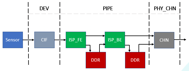
VI is divided into four levels: input device (DEV), image capture device (ISP_FE), image processing (ISP_BE), and image correction (CHN).
Sensor transmits images through CIF interface and delivers images to ISP_FE, which extracts statistics such as AE, AWB, AF, etc., and stores raw files in DDR. Then, the ISP_BE converts the color space and adjusts the image quality of the raw files in either online or offline mode before storing the YUV in DDR. Finally, the backend CHN can perform processing such as crop, rotation on the YUV data.
The parameter configuration of current processor devices is shown in Table 4.1 .
Processor |
DEV |
PHY_PIPE |
PHY_CHN |
VIR_CHN |
MAX resolution |
FPS |
|---|---|---|---|---|---|---|
CV181x |
3 |
5 |
5 |
0 |
5M(2880x1620) |
30 |
CV180x |
1 |
1 |
1 |
0 |
4M(2560x1440) |
30 |
Attention
CV180x does not support HDR.
4.2.2. Video Input PIPE
The PIPE of VI contains the relevant processing functions of ISP, mainly for pipelining image data processing and outputting YUV image format to channels. Please refer to the “VI and VPSS” work mode description in the “System Control” chapter for the working mode of PIPE.
4.2.3. Video Physical Channel
Each physical channel has a clipping function and supports typical resolutions, such as 2880x1620@30fps, 2592x1944@30fps, 2560x1440@30fps, 1080p@30fps, etc.
4.2.4. Binding Relationship
The binding relationship between Dev and CIF is fixed and cannot be modified dynamically.
The constraint relationship between Dev and timing input interface is shown in Table 4.2 .
VI DEV |
MIPI |
SLVS |
BT.1120/BT.656/BT.601 |
DC |
TTL |
|---|---|---|---|---|---|
0 |
0 |
0 |
0 |
X |
X |
1 |
1 |
1 |
1 |
X |
X |
2 |
X |
X |
X |
X |
2 |